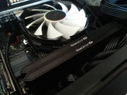
Team Group Xtreem " Edition" 16GB (2x8GB) DDR4 PC4-32000C18 4000MHz Dual Channel Kit - Black
MANUFACTURING DESCRIPTION
Module Manufacturer: Team Group
Module Part Number: TEAMGROUP-UD4-4000
DRAM Manufacturer: Samsung
DRAM Components: K4A8G085WB-BCPB
DRAM Die Revision / Process Node: B / 20 nm
Module Manufacturing Date: Week 13, 2018
Module Manufacturing Location: Taiwan
Module Serial Number: 02024AC8h
Module PCB Revision: 00h
PHYSICAL & LOGICAL ATTRIBUTES
Fundamental Memory Class: DDR4 SDRAM
Module Speed Grade: DDR4-2133P downbin
Base Module Type: UDIMM (133.35 mm)
Module Capacity: 8192 MB
Reference Raw Card: A0 (8 layers)
Initial Raw Card Designer: SK hynix
Module Nominal Height: 31 < H <= 32 mm
Module Thickness Maximum, Front: 1 < T <= 2 mm
Module Thickness Maximum, Back: 1 < T <= 2 mm
Number of DIMM Ranks: 1
Address Mapping from Edge Connector to DRAM: Standard
DRAM Device Package: Standard Monolithic
DRAM Device Package Type: 78-ball FBGA
DRAM Device Die Count: Single die
Signal Loading: Not specified
Number of Column Addresses: 10 bits
Number of Row Addresses: 16 bits
Number of Bank Addresses: 2 bits (4 banks)
Bank Group Addressing: 2 bits (4 groups)
DRAM Device Width: 8 bits
Programmed DRAM Density: 8 Gb
Calculated DRAM Density: 8 Gb
Number of DRAM components: 8
DRAM Page Size: 1 KB
Primary Memory Bus Width: 64 bits
Memory Bus Width Extension: 0 bits
DRAM Post Package Repair: Not supported
Soft Post Package Repair: Not supported
DRAM TIMING PARAMETERS
Fine Timebase: 0.001 ns
Medium Timebase: 0.125 ns
CAS Latencies Supported: 9T, 11T, 12T, 13T, 14T, 15T, 16T, 18T, 19T
Minimum Clock Cycle Time (tCK min): 0.938 ns (1066.10 MHz)
Maximum Clock Cycle Time (tCK max): 1.500 ns (666.67 MHz)
CAS# Latency Time (tAA min): 13.500 ns
RAS# to CAS# Delay Time (tRCD min): 13.500 ns
Row Precharge Delay Time (tRP min): 13.500 ns
Active to Precharge Delay Time (tRAS min): 33.000 ns
Act to Act/Refresh Delay Time (tRC min): 46.500 ns
Normal Refresh Recovery Delay Time (tRFC1 min): 350.000 ns
2x mode Refresh Recovery Delay Time (tRFC2 min): 260.000 ns
4x mode Refresh Recovery Delay Time (tRFC4 min): 160.000 ns
Short Row Active to Row Active Delay (tRRD_S min): 3.700 ns
Long Row Active to Row Active Delay (tRRD_L min): 5.300 ns
Long CAS to CAS Delay Time (tCCD_L min): 5.355 ns
Four Active Windows Delay (tFAW min): 21.000 ns
Maximum Active Window (tMAW): 8192*tREFI
Maximum Activate Count (MAC): Untested MAC
DRAM VDD 1.20 V operable/endurant: Yes/Yes
THERMAL PARAMETERS
Module Thermal Sensor: Not Incorporated
SPD PROTOCOL
SPD Revision: 1.0
SPD Bytes Total: 512
SPD Bytes Used: 384
SPD Checksum (Bytes 00h-7Dh): 5B6Fh (OK)
SPD Checksum (Bytes 80h-FDh): 58B6h (OK)
PART NUMBER DETAILS
JEDEC DIMM Label: 8GB 1Rx8 PC4-2133P-UA0-10
FREQUENCY CAS RCD RP RAS RC RRDS RRDL CCDL FAW
1067 MHz 19 15 15 36 50 4 6 6 23
1067 MHz 18 15 15 36 50 4 6 6 23
1067 MHz 16 15 15 36 50 4 6 6 23
1067 MHz 15 15 15 36 50 4 6 6 23
933 MHz 14 13 13 31 44 4 5 5 20
933 MHz 13 13 13 31 44 4 5 5 20
800 MHz 12 11 11 27 38 3 5 5 17
800 MHz 11 11 11 27 38 3 5 5 17
667 MHz 9 9 9 22 31 3 4 4 14
INTEL EXTREME MEMORY PROFILES
Profiles Revision: 2.0
Profile 1 (Certified) Enables: Yes
Profile 2 (Extreme) Enables: No
Profile 1 Channel Config: 1 DIMM/channel
XMP PARAMETER PROFILE 1 PROFILE 2
Speed Grade: DDR4-4000 N/A
DRAM Clock Frequency: 2000 MHz N/A
Module VDD Voltage Level: 1.35 V N/A
Minimum DRAM Cycle Time (tCK): 0.500 ns N/A
CAS Latencies Supported: 18T N/A
CAS Latency Time (tAA): 18T N/A
RAS# to CAS# Delay Time (tRCD): 19T N/A
Row Precharge Delay Time (tRP): 19T N/A
Active to Precharge Delay Time (tRAS): 39T N/A
Active to Active/Refresh Delay Time (tRC): 58T N/A
Four Activate Window Delay Time (tFAW): 60T N/A
Short Activate to Activate Delay Time (tRRD_S): 18T N/A
Long Activate to Activate Delay Time (tRRD_L): 18T N/A
Normal Refresh Recovery Delay Time (tRFC1): 700T N/A
2x mode Refresh Recovery Delay Time (tRFC2): 520T N/A
4x mode Refresh Recovery Delay Time (tRFC4): 320T N/A