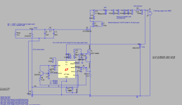
Nick's little project

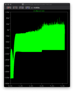
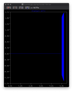
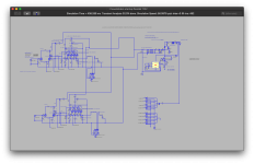
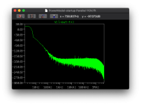
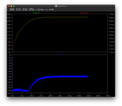
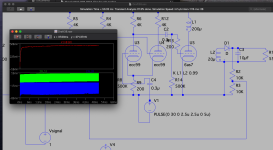
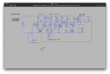
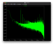
So I have a model running.. this is the last sub-second sample as the amp is just about stabilised.. this is the full amp model - one channel running 30Hz and the other 10Khz to check for cross talk.. there's no cross talk and no noise. The real 24V PSU would have some noise but that is likely to be attenuated by the low pass filters.
XX0WIEq.png
The obvious thing is that the signal is quiet - 447mV input but low output.. need to look at the scaling but the main thing is the power supply.. that's decent enough I think.

No if only I can get this into a proper power supply.

There's an evaluation LT3751 but it's unlikely to be able to provide the current required for the entire amp and the eval board is £100, it's pretty steep.
 
Actually an update :)

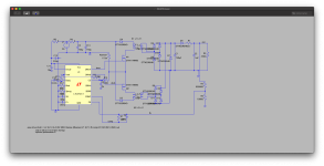
I built the bill of materials but was concerned about some aspects of the LT3751, so switched from being an isolated flyback to a non-isolated boost and instead using an LT1243. The system as a whole is isolated - I'll be using a 240Vac-24Vdc medical power supply hence it has PRC and isolation. So any lightning strikes or general bad transients will have to get through that first.

The problem was around the power transfer per pulse. In short the LT3751 is designed to give it a load then keep a cap filled by running a regulated Topup. The issue becomes it can't provide enough power overall due to it being a fixed frequency and waveform.

The LT1243 is dumber, it's a PWM chip that has feedback (ie use the same output voltage feedback), current limiting (on the mosfet source side) by blanking pulses but has a couple of interesting points - it supports up to 1MHz switching and secondly the oscillator is controlled by an external RC (resistor-capacitor) so it gives some crude ability to set the shape of the pulse and the frequency of the pulse. This means the parameters can be adjusted for load.

The importance here is energy per pulse. Too fast and the inductor doesn't have time to build up a flux field that's big enough boost the voltages. Too slow and the switching becomes auditable. Then the shape - a sawtooth shape is good for noise (less steep vertical changes in voltage) but taking a rectangle (max wave form) and cutting like a triangle means 1/2 the energy per pulse. Lastly is the blanking of power - this is when the system is idling and the PWM chip simply cuts the power to prevent the voltage from rising further. The downside is that the skipped cycles act like a lower frequency so they quickly end up into audible spectrum as noise (along with the harmonics).
Now an ideal system would work at the lowest power (ie smallest number of pulses with the biggest gap between them) but be above the audible spectrum, say 50-100KHz, then have waveforms that are a trade off of power vs noise. The result is then the noise is always above the audio spectrum and therefore can be filtered effectively.

Without resorting to custom programming of CLPDs, or more expensive PWM chips (think expensive frequency generators) this is probably the best option.

So the full amp model has been running with this, a few tweaks and it's looking promising - I still want to perform a couple of additional runs for full 3.16V and 0V input but this is 445mV. That way I can guarantee the amp will not start buzzing as it starts skipping pulses at 0V input (ie quiet passages of music) and still support the big transients if need be.

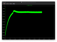
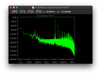
Time period 7-9.2 seconds from the startup:
VXTJ9xt.png

The 10Khz left side signal is good, but you can see some cross talk from the right side 30Hz signal. I still have some work but the noise level is starting to be acceptable.

Now to the good point...
GQX2W2A.png

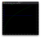
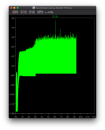
This is the 24Vdc supply current. Simply put 6A * 24V = 144W and that's the spikes so in reality it's probably averaging less than that.

I'm not sure how LTspice works out it's current but the -14A would probably be the initial inrush for the caps not a problem, if I was to use the 300W 240Vac-24Vdc isolated PFC power supply.. that supports 14A so this is looking good as the power supply is reasonably efficient compared to a linear PSU. Add to that I'm using passive low-pass-filters (ie large caps) then this is looking good. This also makes the building of the 'device' a little easier as we don't have 40A bus bars and it's easier to find/use <20A current wiring.

Once I've checked 0V and 3.16V (ie lowest power draw and highest power draw) then I'll be interested in making up the new BOM and cracking on with the ordering and PCB design.. which should be relatively close to what I had in mind before.

I've also decided that rather than run a single large SMPS that runs the heaters too - I'll use one for the B+ and one for the heaters. The reason is regulation - if the power levels/pulse rates change for the B+ PSU they'd also effect the heater currents/voltages too. Given the price of a 100W 240Vac-12Vdc (can be adjusted to 12.6 and has a 0.15Vpp ripple) is the same as a 24-12 converter of the same standard.. it's a no brainer to simply have the two SMPS and tie them to the same power on/off and power mains socket.
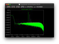
 
Ok 3.16V results are good.

Not much more power consumption, so still within the 300W PSU capability:
Ry4t6Mt.png

Outputing some serious power (headphone wise) - this has since got to 2.5V:
bGXfNRo.png

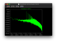
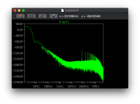
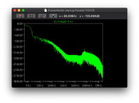
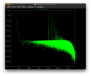
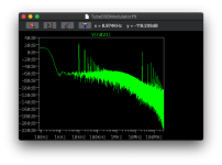
And the noise 7.8.2s (so a second less than the previous FFT):
TvgV53b.png

That 3.15 is +20dBV, so beyond normal playing and only for transients like cymbal crashes. Given you'd be deaf at this point. 2.5V into a 104dB/V means uncomfortably loud at 108dB .. the poor headphone coils would be melting. (+3dB for every 2x volume). That is a decent noise level.

100dB is the range of a most people's hearing.. 120dB is the point you'd become deaf through ear damage almost immediately.

The reason for this test is to look at the distortion (ie the harmonics) caused by clipping.. there's a lot in that so.. we have some amp tuning todo but the power is available which is the purpose of these models.

Next will be a 0V input and we can then see the pure noise from the power supply.
 
Found that version of the power supply had a problem with blanking and sub-harmonics.

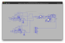
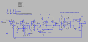
I've now replaced the MOSFET with a 900V 20A piece (the SMPS boost topology needs 2xVout at least on the switch). The system seems decent so I'm running it on the amp model.. It's slow but then the size of the model looks like this:

YBg20wP.png

The updated SMPS mosfet is a biatch, being sensitive to noise and other instability effects - so the SMPS now has three snubbers to remove noise - including a resonant snubber around. the SMPS inductor - this recycles the switching spike so it's more efficient.

Running slower initially about 40KHz but this could do 1Mhz given the mosfet is a fast device (ie tens of nanoseconds switching).

It also seems to output ripple in the order of 0.5-1mV.. based on the initial test. Let's see the noise output on the large amp model.
 
Output at 0.8s simulated.. still starting up, at 90V out of 150V for the output tubes but this is the noise level at the moment:

ZRGqTrv.png

So fingers crossed it stays this quiet and no issues :)
 
So I've moved on from the simple boost converter. *monty python*it is a silly topology* and the junction temps I think were causing a problem.

I present - the hybrid.. actually it's a push-pull half-bridge controller but running two flyback converters with full bridge rectification on the other side. This means each converter (and mosfet) is only running at 1/2 power.

Typically transformers are a pig to find, so I'm using a hybrid to make the choice of transformers easier and provide more power capability. Typically boost and flyback stop really working about 200-300W as the mosfet junction temperature and other components start becoming cumbersome in finding and expensive..

I've switched to using this controller: https://www.analog.com/en/products/ltc3723.html

Here's the initial attempt at a design:
KuhCxRg.png

This us using two 20A 500V capacitor charging transformers - so they can cope with the load but they have a switching limit of 50Khz, so by running two alternately I get 100Khz (actually 144KHz) so the shapes the noise and keeps it up in the spectrum:

Currently the model is about 70V, but it's looking good:

fGuY7kv.png

fqMSwtJ.png
Blue is showing about 7A of 24V supply.. which is about 170W. So there's still some tuning.
 
Ok, around the houses including looking at alternate half bridges etc but I now have a 600mA @230V capable boost converter from 24V that is simple. Turns out having large caps means large upkeep per cycle which is not what an SMPS likes (unless you use a different topology):

I11onVW.png

XflT8sa.png

Next up is to see how this behaves in the large amp model.
 
So on powering the main big amp model at idle:

A1xZ11v.png

~70W for all the tubes B+ needs. The supply will give 600mA at 230V from a boost converter (single mosfet but dual inductors). Add ~30W for the heater supplies and we're cooking.. err almost there!

Being class A when the amp starts amplifying that load may increase.. no problem that SMPS will be 300W capable (actually it's 336W).

I still need todo some additional modelling but the noise isn't too bad. This is period 4-6sec after startup from the B+ of the output tubes.

T8BeQjb.png

Not bad, the noise from the SMPS is way up at 60-100Khz+ range. Although tubes can pass/amplify that frequency. The low end noise is simply the amp still partially charging over the sample time.

In short, the SMPS approach seems todo very well so far. Just need todo a full 3.16V input to test the maximum power use.


So the cost... well the components aren't too bad. I'll buy the 240Vac->24Vdc SMPS asa OTS, but the major cost of the booster are the inductors £36 for two and £28 for the MKP caps on the output. Unlike the old linear PSU, this only has a 80uF and 20uF 800V caps on the output, but has a number of 63V 330uF low ESR caps which are ... 78p each :D

I still need to check the main amp, as I use some large 450V caps (350 and 750uF), plus on advise the output caps are 2200uF and I'm thinking that those may be overkill (or at least they could be paralleled for lower ESR).
 
Last edited:
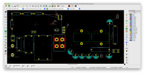
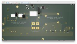
The power supply booster PCB is coming along nicely.. things get large when you're throwing power around.. currently that's 240mm x 120mm but it can be optimised.

4vB2Dto.png

The above is not complete, nor is it final.. the weedy tracks are simply there to get my head around things - most will be removed for area pours.

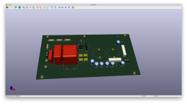
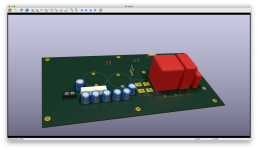
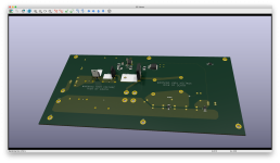
I have some of the components that have 3D models.. so it gives an idea of what it will look like:

B0Fyhj6.png
 
Last edited:
Modifications, corrections and progress..

qhzvOBB.png

o6nlRJL.png

There are some limitations - the inductors are 7A max each so 14A of 24V is the max, the power supply I'll use is about the same around 13-14A max, I've set the current sense (that's large 4 pins in the centre) to limit at 13A so it's a cheeky 75mOhm 100W capable using a heatsink. The idea is to have a heatsink bolted to the side with the mosfet (ie the side with the IC chip) and then bolt the fet, diode and output resistor onto it. The average wattage is actually quite low, probably about 10-15W of heat, so the idea is that it can be convection cooled using the heatsink.

I've tried to design for maximum voltage clearances and maximum current track thicknesses. In the end there's limitations given the device pins are only a certain distance apart before bending. I tried simulating the design at full 24V almost 14A current average input .. ie 300W.. the output was 750mA at 270Vdc output (202W output!). 60% efficient which is better than the linear PSUs. That's probably as much as you realistically want todo on a PCB before thinking about thicker bus-bars. At that stage it's probably better to step up to 48V but that would need some changes for the IC chip (25V max).
 
Given the shortages for the components I think it's time I started ordering the bits, it will several months assemble the bits and then I can put together a little test setup with croc clips.

Updated version of the board uses the correct sizings of traces - I need 7.68mm of 2oz for 20A to keep to a +40degC heating effect. In reality the inrush will be at max 13A and operation will be in the order of a 2-3A but this means the board has very low impedance and I won't cook the PCB tracks on startup (unlike my MF A220 which has darkened PCB tracks!). I've also spaced the pins on for 900V - normally this wouldn't be an issue but over time I may want to make a higher voltage model so the transients may end up being higher.

bm1cmpH.png

Looking at prototype board manufacturers - given it's about 240mm x 120mm and 2oz traces - the UK is quoting £250 for 1 and china is quoting $187 for 5 boards. If the board works I can always sell off 3 in the DIY tube-amp community which means $37 per board. There are possibly some design modifications I can make to reduce the size - however given the size of the components, that's difficult.
 
So I have an idea of how the board could be made smaller with less EMI - the board above has open inductors and the power and return lines are aligned separately, where instead the lines can be run stacked above each other IF there's enough separation for the high voltage. The issue here is that separation like that means prepregated layers and we're talking a complex manufacture. Also resin is susceptible to cracking so the board may fail over time.

I think though it would be possible to improve the layout and use shielded inductors but still get the performance required with less radiated noise and smaller dI/dt loops.
 
Currently running a full simulation with the boost converter and a maida LT3080 regulator.. The output of the Vripple regulator currently 1mV. Or put better 0.001 volts. Although with some tweaking that could be reduced - I'm targeting around 20uV, or about 100dB noise floor.

VFxAVNf.png

The simulation is just about 2.5 seconds in after running overnight. but the noise performance seems good (although it's too early to say just yet as it's still starting up in the simulation - so need a good 5 seconds)...

2a79Dir.png

That's spicy appetiser!

The dB scale is logarithmic. which has me a little puzzled as my previous modelling of the regulator and booster by itself has shown a 1mV ripple, but is modelling at -80dB for the frequency spectrum.
60dBV = 0.001000V (1mV)
80dbV = 0.000100V (100uV)
100dbV = 0.000010V (10uV)
120dbV = 0.000001V (1uV)

So this is looking like the system is running at 10uV ripple or thereabouts, so I suspect the current draw (it's not at max yet) is helping lower the noise floor. I'll need to wait to see. This is with a model that has a power supply input of 24V with 150mVpp ripple.

Nice... it also means the amp supply will be stone cold silent. Only the noise of the amp (tubes, resistors and caps) or the music will be appearing through the headphones. That's assuming the EMI radiated noise can be kept under control.
 
Last edited:
Hehe ... some updates :D

1. My amp is now about 0.8% THD and there's still some tuning.

2. My SMPS boost is looking good - managing 160W.

3. I've started looking at a Tube SMPS-Class-D output section :D

vezxCUi.png

That's self regulating at ~ 500mV from a 200V input using a 200Khz pulses :D without using a mosfet...
 
Hehehehee Class D in tubes.. so that's Class D amplification implemented in vacuum tubes using a 200kHz switching rate.

wt3tGQy.png

A 100Hz input signal.. and we get all the noise of the tubes (harmonics too).. but that's damn good

2VNu38R.png

Not bad for a first attempt! I still need to check if I'm not doing something daft but if that's correct then that's quite cool :D
 
Update time.. so ideas have moved on:

FTeRIQX.png

So the above is one channel of the analogue to DSD512 direct digital amp :D No solid state.. just vacuum tubes. It's pretty much where I was headed, so I thought you know what.. why not.

The front end valve (left most) will probably be altered to be a slightly better analogue section. However this uses VHF valves running at about 22MHz then runs the power output valves (right most) to act like a digital amp. I can change the back end to mosfets, even (as planned) to switch 390Vdc.. In theory this could run headphones or even a KWs of power amplification.

So DSD is essentially a form of Pulse Density Modulation (PDM) related to PWM but has some advantages - all the pulses are precisely 22nanoseconds (ie 22Million/second) or 512x the speed of a CD. So unlike PWM it doesn't create noise across a wide spectrum as easily.

Here is an FFT - you'll see the 10kHz sine wave plus harmonics, but also the 22MHz switching noise. It's 60dB because this is literally about 40mS of simulation time, given longer run time that should drop down nicely.

sfca5ci.png
 
Think of an analogue to digital converter that the uses a power digital to analogue output.

You plug in your record player.. and your speakers. It’s just the bit in the middle that’s complicated. To make it more complicated still.. there no solid state chips.. just old school 1940s vacuum tubes doing everything.
 
So I've been focused on the front end of the analogue V1 which has some hardcore power requirements - 640V split +320 to -320. Incidentally this is the same power requirement as the tube op-amps. So if I solve this, it solves a piece of the puzzle for the direct digital amp.

So I've spent a little time re-looking at linear power supplies - the problem is that off the shelf only sit within two domains.
First being the 240V and below, this gives a potential of 390V full bridge rectified (input AC RMS *1.414 for peaks) but has the disadvantage of 60% current. So using voltage doublers and the like then end up in multiples of 110V for example and if you want something above or below that's a large use (and potentially 100s watts of heat) resulting in larger AC transformers.. which in turn means more heat..
Secondly 'bespoke' transformers for high voltage tube amps - these you can get but they don't provide current. Thus I'd need one for the 320-0-320 (60mA) and one for the 200-0-200 (500mA). Sounds simple but finding a 400V 500mA is a problem. In theory two 200V transformers in series could work but they have to be identical. Multiple transformers, not entirely fitting power requirements = multiple sets of resistors and voltage regulation resulting in even more heat.

This means that you end up with a rather large, heavy, very hot power supply. Plus todo that properly. without being grossly inefficient, you need to have transformers built to specification. Macintosh I am not (they wind their own transformers).

So that got me thinking back to the boost converters - I've been focused on the Cuk converters running CCM to provide the two boosts - 390->640V (giving 320-0-320) and 390V->400V (giving 200-0-200). In fact these would be the same design - literally with slightly different values of components on the same design PCB. Secondly linear suffer in not being regulated, so as the mains supply can vary as much as ±10% that's a considerable change in the power and thus operating points of the tubes (it changes the designed points on the load line). Regulating linear means you need additional voltage and current.. and so you may as well go SMPS as this does all of this.

I've been exploring CUK CCM converters that are isolated. The nice thing is that going from 390 to 640 needs only a 40% CCM duty cycle so there's less chance of instability as you go into 50-100%.

CUK is interesting - a capacitor essentially separates the two sections of power in an unisolated CUK. Instead we're using a coupled inductor or transformer - here in lies the rub again.. they are all designed for sub-48V or 1:<1 with very few providing step up capabilities. So for an off the shelf we're looking at a minimum of 1500V isolation, preferably 4000V isolation - this is because of the way boosts work. Again - I'm trying todo this with off-the-shelf parts.

A CUK boost works by using an inductor (let's ignore the other topologies) and uses the inductor property that it doesn't like changes in flow. It's todo with the flux - as the input current flows through the inductor and through the closed mosfet, it builds up flux, then the mosfet is switched off to open the circuit.. the flux then pushes forward onto the capacitor, causing a higher voltage (the boost) on one side of the capacitor. The other side then sucks more electrons (corresponding to the boosted voltage) through the diode. The mosfet switches on and the voltage drops, the inductor builds up it's flux but the other side of the capacitor has only one way to go.. through to the load.
Now there's an inductor to smooth the spikes out on the output side, along with a smoothing capacitor.

An isolated version of this can either - (a) use coupled inductors instead of direct or (b) use a transformer instead of the load without the need of the primary side diode (thus the big swings appear on the transformer and thus end up on the secondary side).

The entire system works in a closed loop - so it looks to keep the load at a specific output voltage but also limits the current through the mosfet per pulse. The benefit is low ripple and noise - given this can be put into the kHz or even MHz ranges. MHz - well that then means we're looking again at a step to the full 30MHz digital system. Again another piece in the puzzle (although I will probably switch a 48Vdc supply for the digital amp).

So I have an initial design on this, I've been exploring options in terms of boost controller that supports MHz switching. The previous straight non-CUK boost performed 24V->390V but this is a different beast but offered some learning experience.
 
So I've started ordering for the V1 amp - this is the M60 front end and a push pull OTL backend running in class A.

So I'm ordering and some of the components
* 16x (one channel's worth) Nichicon ES Muse 50V 330uF caps for the output capacitance.
* WIMA FKP4 630V (400Vac capable) 0.1uF caps for the internal capacitances.
* 16x B9A tube sockets.
* 600V 20AWG solid wire
* tag boards
* solder
* resistors and bourns variable resistors for tuning

The Nichicon ES Muse is a a bi-polar electrolytic and as long as you're using low voltages remains a very good audio cap (not your grandfathers electrolytic). The good news is that the headphone output is low voltage and lowish current too. Hence the selection.
To increase the frequency response - these are placed in parallel for each of the paralleled OTL output triodes. So that means for each push-pull pair there are four bipolar output caps in parallel with a smaller bypass film cap. A total of 16 Muse caps per channel (5280uF) which is over kill - I may reduce this to two or three per PP pair (2640uF/3960uF) depending on listening experience.
The amount of capacitance is not for energy storage like a power cap (ie there's no point putting 10,000 or 150,000uF) but is used to block the DC from the output headphones and only allow the AC signal to the headphones. The capacitance is used to ensure both low ESR (lower impedance) and thus has better low frequency performance at higher currents. Think of it as a bigger radiator to transfer heat in your house.
Normally you'd use a film cap but the physical size of a cap would be about the size of a briefcase thus using a bi-polar electrolytic is a good compromise.
Why bi-polar here? Well an standard polar electrolytic can only cope with current flowing in one direction (think of a rechargable AA battery where one battery plate can only cope with it's respective polarity charge). A bi-polar is built so that it can cope with current flowing in both thus mimicking a film cap (internally this is normally done with two matched electrolytic caps as part of the design).
For audio - the output signal current flows in both directions and for a push pull totem topology, the voltage applied to tube side can be both above and below the current voltage on the output. Thus a normal electrolytic would deteriorate or even destroy itself.
A 24V TVS sits on the tube side.. this safeguards the caps from being exposed to larger than 50V difference. In the final amp this would cause a latching crowbar to cut in, shutting down the output stage and reducing the current to zero until it's reset.

The WIMA FKP caps are non-metalised film caps, unlike the Panasonics. The pan caps are good and cheap (about 30-40p each) with decent performance. However metalised caps have a little more third order harmonics (although you'll not probably hear that it can caused additional effects in a long chain of tubes). So I've decided to go for non-metalised. This means the capacitance for size is lower as the internal conductors are thicker but the result is better current handling and less distortion.
The FKPs 0.1uF is 2.5x3.0x1.5cm and about £2 per cap. So I could use a 0.3uF or a 3x0.1uF in parallel. Essentially my thinking here is that £6 is acceptable.. vs something like the lovely Auricap XO 0.3uF that's about £24 each! Not only that but given the WIMA quality management.. the resulting caps are within 5% tolerance - making matching phase and channels easier!

I will order metal foil resistors today along with the other components. Carbon comp/film result in noise from current through the construction (although carbon comps fail open like a fuse) - this works for low current tube amps but not for OTL output tubes.

Once I have the pieces I can finalise the layout - there's no point putting the components in and not factoring the spacing to minimise wires.
 
Back
Top Bottom