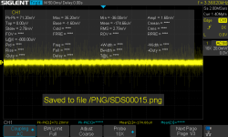
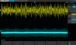
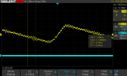
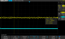
Nick's little project

Still waiting on the third back-ordered transformer. Other priorities have got in the way but all 5 power supplies are built point-to-point. Each supply is a RC to RCRC filter with a 1.5mA capacitor bleed to discharge the capacitors and a red LED indicating power on the capacitors. I have some body work todo for mounting points which should be done later today. I've ordered a few additional components to protect the amp power supply from transient voltage spikes (MOVs), an 68 Jule NTC (which helps control inrush current) plus some big polarity protection diodes the polarity sensitive electrolytic caps for each of the power supplies incase they switch off at different speeds. This is possibility given the power supplies for a circlotron are stacked. The neon power switches work nicely, so the next step will be to get the power supplies mounted, connected up and test the startup/shut down without the amp being completed.

The 117Vac power supply outputs over 170Vdc, this is due to not having any load. However given high DC voltage is extremely dangerous I've also ordered some multimeter clip leads I can clip on before powering up rather than having my hands inside when it's running. Once the low voltage supply transformer arrives, the high voltage will sit on top of the 30Vdc of the low voltage power supply - so 200Vdc. The capacitors in the high voltage supply bleed quite quick (being only two 390uF 350V caps) and the low voltage power supply bleeds slower (two 5600uF 50V caps) and the heater supply has a whopping 30,000uF 25V caps as it's only providing 12.6V. All the supplies have their own transformer secondaries so they are independent and float (this is important).

The design of a circlotron is simple - two amps, each side of the speaker/headphone speaker has an amp. If both amps play the same thing then you get zero difference and no current flows through the speaker. If both amps play the same thing but opposite then you get 2x the current flow of a single amp through the speaker - think of it like a seesaw, one amp at the bottom and one amp at the top and the slope of the seesaw is the current flowing - the steeper the slope the more power is being delivered. The same is true for the circlotron. The headphone is the seesaw and the two amps on each side (bridged essentially) are providing that slope.
The complexity of the circlotron is the supply of power. Each amp has it's own power supply that floats to provide the same power regardless of where the amp is on the seesaw. A hybrid (tube+solidstate) circlotron is two power supplies per amp. A high voltage for the tube and a low voltage for the solid-state components. So these two floating power supplies of each amp move up and down with it on the seesaw.
Tubes provide a further complication with heater supplies. They need to be within a certain voltage range of the tube cathode as they are so close over 100V may cause an arc and destroy the tube. This fortunately for our headphone amp can be referenced to ground. The sine wave we create is less than 5V so the cathode will never be more than ±8.3V (5V+12.6/2=8.3V) from the heater voltage - this is because pivot point of the amp is centred around ground..

So if everything is floating how is it a seesaw?
Well the pivot point of seasaw is the same in a circlotron. The centre point of the two amps is connected to ground (zero volts) thus both amps pivot around 0 Volts. The connection go the speaker is connected either side of the pivot point (ground). So the slope always goes through 0 volts in the centre.

Given the amp is connected DIRECTLY to the headphones - the headphones are essentially connected between 200V and the largest signal in the event of two shorted tubes could be 400V. However shorting tubes can be safeguarded by detecting over current - the 12BH7A is 20mA max and shorting occurrs in most tubes either as (a) heater element failure and shorting to the cathode with is not a high voltage issue or (b) if the tubes are run so hard beyond their maximums that metal in the tube vaporises and condenses on the elements causing a short.
This circlotron is a a cathode follower with a emitter follower linked to the cathode, a short will pull up the voltage but it's possible safeguard by limiting with a TVS diode or a pair of Zenner diodes to clamp the maximum voltage. The result would be a limit of say ±5V to the headphones the diodes would open, causing current flow and the fuse in power supply would burn out. A shorted tube is dead anyway and there would be a possibility that you have a very hot BJT transistor for the split second before the fuse blew. The BJT base to emitter voltage could be clamped by a diode to prevent this "max current flow" thus saving the BJT too.

It's also possible to have the mute relay drop and lock should this occur - physically cutting off the amp from the headphones. This mute would be required on startup anyway. For now I will be using a 5W 55 ohm resistor as a speaker substitute to measure and test behaviours. I have a 2W 50ohm speaker for the next step - is there sound etc, although the oscilloscope can show how clean the sound is. After a lot of testing and a few more safety tests.. then I'll add a headphone socket and add the headphones.

This isn't a build from a known and tested schematic.. hence the very experimental approach.. and the fun.
imVysaj.jpg

So I hope to be able to get the next chunk of work done this weekend. Enough to power up the tubes whilst I wait for the back ordered transformer to arrive..

I ordered some 1000V multimeter test clip on leads.. that way the multimeter can be connected up before power up without needing to get my fingers and a probe too close.
 
Last edited:
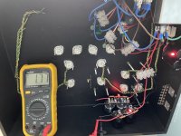
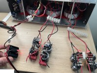
So I have the power supplies built, tested and then the power test configuration setup:

zcRSYMd.jpg

~175Vdc from each of those two power supplies - for tube B+ power. The small supply at the side is of heater power supply it's current reading 16V which is a bit high so I will have to drop the voltage.

The circlotron benefits in that it cancels noise from the power supplies:
nhIDg8O.png

So 175Vdc and that resulting after both supplies cancel out ripple is ~25mVpp or -90dBV. Not bad considering it's a RCRC filter without any regulator etc.

I've had issues with the neons in the switches causing short circuits - blowing one of the 1A fuses through toroidal back EMF, the main 3A Live & Neutral fuses blew due to the switches and the current draw on restart for the heaters supply (30,000uF) blew one of the 1A fuses. The joys of tortoid transformers - better efficiency but so they also become more tricky- especially in parallel!

You can see each power supply has a diode to show if the caps are charged, they slowly dim once the power switches off as each has a bleed resistor.

This is not the final wiring, but simply to get things working and test before we start on the tubes.
 
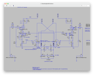
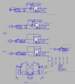
From this schematic:
UKrGPIM.png

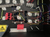
To this wiring layout:
826u02U.jpg

To this:
ZxmxT0S.jpg

I am still waiting on the low voltage power transformer. Until then, I'll not bother installing the hybrid NPN BJT transistors for now.

However for now I can test the tube side. If I use my 8 ohm 100W resistors in series and use a pair of 10K resistors in parallel then I can drop that 16.64V down enough to keep within the 12.6V heater voltage ±1V heater tolerance. I can then test the tube side of things such as tube bias, the DC servo, the Bit bias etc before moving to test a signal through the tubes. For this the 55 ohm 5watt resistor will be the load (that's the aquamarine coloured resistor in the middle). I suspect it won't have enough oophf without the BJT to provide the 50ohm 2W speaker but that's a possible option to try after.

I'll have to give the amp a clean out - that dust is from the build with the solder balls that spit off the solder.
 
foFwhKp.jpg

8lzjRNb.jpg

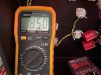
The milli-volts across a 10R resistor, by dividing by 10 I get the current through the tube - this is 8.5mA which is close to my 9mA design. The heater voltage is a little low as I added 16R into the voltage but instead I think I can take that out to get to the 12.6V.

This pm I'll get the scope out but for now that will do :D
 
Last edited:
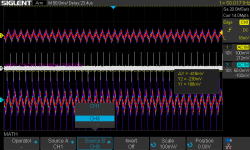
So after doing a lot of poking with the oscilloscope, it's obvious that the bridge rectifiers have a load of ringing noise.

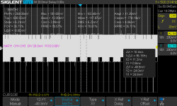
First - looking at the noise remainder from by subtracting the two sides of the amp and then ignoring the diode switching spikes by using the cursors:
dFxMKRQ.png

48mVpp of noise. Not bad, if my calculations are todo that's -108dBV. No fancy power supply just yet to combat the noise.

It's way to early to try this - the tube is only putting out a very small voltage and as the BJTs aren't in place there's no current being driven (or LV power supply todo this). The tube is running at about 160V, and 8.7mA with a 8R in the heater circuit.

RCf8FoV.png

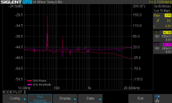
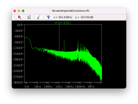
You can see the frequency response is going to be pretty good - the spike at 100Hz and the spikes up are due to the diode noise and it's respective harmonics. The low output of the tube shows up as a low amplitude of the frequency response. In theory once the BJTs are in that will go up in scale but the shape will remain the same.

And this is one of the switch events - the benefit of a oscilloscope is being able to see and characterise it:

LA5LZdM.png

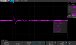
You can see the rectrification diode switching and the ringing (the undulation) caused by the transformer and the diode interacting. A snubber (resistor+cap) across each should remove that switching, but calculating is tough. However once it's sorted that's it and it shouldn't be a problem.

So happy with today - the startup went well, there's a few issues but as this is designed from scratch I'm not surprised.
 
Update - focusing on noise and the rectification (converting AC to DC) noise (spikes).

The power path goes:
1. Mains AC plug - fused

2. IEC Mains filter - fused, switched, and common mode choke filters to reject EMI noise through the mains

3. NTC inrush limiting - Toroid transformers have a large inrush of current, over about 400W toroid that's enough to cause it to blow fuses and trip breakers. I will have five toroid transformers in parallel making it an inrush monster. The NTC cold provides some resistance to the inrush (a split second required) and as it resists it heats up and the resistance drops. I have a bypass switch that then takes the NTC out of the circuit and lets it cool down for normal operation.

4. Fuses - these are 1 amp fast blow fuses with a 4 amp fast blow for the heater. I use fast blow now to assess the inrush but I will change to slow blow lower value at a later date.

5. switch for high voltage - this allows the tubes to be pre-heated before applying the "B+" 180 volts across them. Applying the B+ before the heater reduces the life of the tubes. The reason why is that the heater filaments take 20 seconds to reach full temperature, the solid state B+ supply tales 0.2 seconds to power up to full voltage. Old power supplies used a tube rectifier that slowly ramped up the B+.

6. Toroid transformers - the reasons for selecting toroids is their low flux leakage hence they don't hum and they don't make as much EMI as the cheaper square block EI transformers do. This means they're more efficient (smaller for same rated power), but that coupling allows more noise through from the mains and the low resistance means higher inrush.. Each toroid takes the 230V AC (measured on my place as 245V) and then drops this down to a lower secondary voltage. The transformers I have two independent secondaries each. One transformer 117Vac, another 12Vac and the other is 22Vac - note that this is RMS (root mean square) not peak.. but I'll discuss that next.

7. The next step is bridge rectifiers - these convert AC to DC. However the DC goes up and down at 100 times a second - we convert both top and bottom of the AC wave at the mains 50Hz so we get 100Hz, but then we need to make this more steady or we'd just hear a loud hum.

6. RCRC filters - these use the 100Hz bumps to fill up the capacitors, the outgoing power draw by the amp is then kept more stable and the waves are flattened from 117Vac*1.414= 165Vac peaks to about 160Vdc with smaller "ripple" bumps. Those need a but more work but that's better than nothing and allows our system to work well enough to start functioning. RCRC stands for resistor-capacitor-resistor-capacitor. We see a noise level of about a 1V from the 1V ripple. In headphones with 104dB/Volt sensitivity that's a loud 104dB of mains hum.
I'm ignoring the tube heater filter but it's less important for noise reduction.

The RCRC filter won't be the only noise reduction needed but for now this will do.

Now comes the mind bending bit.

If you have the following you can cancel out that large ripple and most commonly shared noise caused by the almost identical power path:

Toroid secondary #1 -> PS#1 -> RCRC#1 -> AMP#1 -> headphone speaker <- AMP#2 <- RCRC#2 <-PS#2 <- Toroid secondary #2.

What remains is the noise unique for each path. This is essentially the concept for bridged amps where you can have twice the power (naturally you have two amps) but you can lower noise if done correctly.

So this is what I have been working on - reducing the noise.

DJfGCwo.png

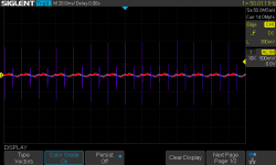
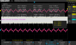
You can see the noise as the multi-coloured line, the spikes are also noise but these are specifically caused by the switching of the bridge rectifiers (step 7 above) as the AC wave crosses 0 volts at 100 times a second. This is compounded by the toroid low resistance and causes it to "ring" (the last photo of my previous post). This is actually the output of one of the amps.

By twisting the AC power cables together it reduces the electromagnetic noise radiated, then by rooting the noisy cables away from other cables (called 'cable dressing') this reduces the general noise as seen as the multi-coloured line. That line has both the residual mains hum from the RCRC filters and the hiss caused by all electrical components as power moves through it (and tubes aren't the quietest thing).

Now let's reduce the diode switching noise using a something called a snubber. This is extremely complex to mathematically calculate or model as each transformer and bridge is different. Instead we can use a variable resistor in the snubber and watch the effect on the scope in real time.
A snubber is a capacitor (blocks DC) and a resistor (increases resistance to AC) across the transformer secondary. So we're working with 175Vac peak (as my AC mains is 245V AC everything goes up in voltage) so we need to be careful. The oscilloscope is running 10x probes here and AC coupled so we see the voltage reduced by 10x and only the moving part of the wave and not the DC to make it easy to watch:

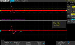
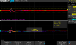
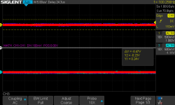
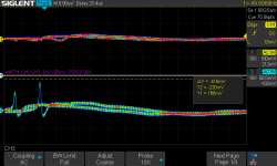
Here's the ringing, and you will see over the next few pictures as I turn up the resistance using the variable resistor in the snubber. These two waves are the outputs from the two sides of the headphone speaker (ie output of each amp):
lYDMdeJ.png

lYDMdeJ.png

8Y1dgWK.png

dHY0Fw8.png

And we're almost there...

3VPyhJh.png

Now we zoom in again:

vhzWjh9.png

You can see that the snubber is only over one of the toroid secondaries - the second doesn't have a snubber (lower wave) hence the noise. As both have a bit of a cancellation effect you see it reduce on the other amp output

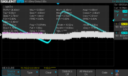
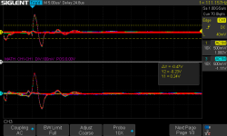
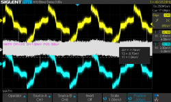
What does that mean? Well it means we see a marked reduction in those spikes - not total as we're not apply it both amps at the moment (but we will later) - the top is our snubbed amp and the bottom is out snubberless amp output, the centre white is a subtraction of the two (ie what you would hear):

99bntI5.png

No spikes on the top trace! (note the bottom trace is zoomed in 2x scale to the top one). The remaining multicoloured noise is our RCRC output with the ripple (the big waves) and the electromagnetic interference that's making the ripple a larger noise (over ie in the MHz range). The scope is able to run at 200Mhz so it will show the inaudible noise picked up from the environment.

Removing a snubber across the PS input this improved things further:
7twF0Mo.png

brMl48n.png

Hmm nice.. the unconcealed noise is down to 1.74milliVolts (0.00174 Volts) which is good but for headphones that will still be an audible hum, instead we will have to add a regulator for each power supply to drop the noise level further - the best would approach 2uV (0.0000002 Volts) which would give a very low noise level and a silent headphone speaker. However for now, and until the backordered transformer arrives, I can live with that as this is an experimental amp design (actually more a sub-unity current buffer to be more correct). The fact we have a tube in there will limit the noise level floor anyway but I'm not too worried about that.
 
Last edited:
So I've attacked a speaker for the first time - this is 50R speaker (rather than risking my headphones) in parallel with a 55R load resistor (making 25 ohm). The speaker is a 2W and lowish sensitivity but more importantly is away from my head.


As expected there's mains hum as shown by the oscilloscope and shows there's a need to reduce the mains hum. No sound through the amp yet - the small milli-amp swing from the tube amplification (the cathode connection means no actual 1:1 or less anyway but lower distortion) I'm waiting on the BJT's low voltage transformer to make the additional current to get over the noise of the transformer hum.

The LT3080 voltage regulator I have in mind is about £5 each for the regulator surface mounted chip without the MOSFET and would drop the voltage by 15-25V across the regulator in the "Maida" design. That would give low voltage ripple and silence. It would make sense as they're PCB surface mounted to simply put the RCRC filter on there too. The voltage drop concerns me a little an I may look to see if it can be dropped less given I'm regulating from under 0.1V.
I could go with a LM317 regulator, cheaper but has all the same requirements for the high voltage (ie needs to be in a maida design with additional components to cope with the high voltage).

As regulators don't cope with high voltage, the maida design creates a bubble of 10-20V under the ripple peak and then sits the voltage regulator in there below the ripple minimum. It then regulates the voltage out providing almost no ripple. Additional components are required to prevent the 175V hitting the regulator at the startup and shutdown which means using a big MOSFET (think 950V 10A capable that can take high current at 200+V for a period on startup to the mosfet will blow itself off the PCB and across the room). Needless to say it's difficult.

I'm pretty much stuck now until the backorder ships. I did also use the scope to sense the EMI in the chassis - there's about 2-3 inches of the transformer-rectifier connection that's an EMI hotspot. Hence it would be good to have that at the top.
 
Looks like the main mouser catalogue entry for the low voltage toroid shows "Expected 11-Jul-22" so I assume my back ordered transformer is in that shipment and thus, shipping US to UK means 5 days so next Thursday/friday or the week after.

One of the nice things about oscilloscopes is that you can use the probes as a EMI (RF interference) probe. I can see the room has a lot of 50Hz EMI and the chassis walls have little to none, but the AC inlet wires and the transformer-rectifier wires create a massive amount of EMI to anything within a couple of inches - such as other wiring that induces hum/noise. Even with twisting the lines together to reduce EMI it's causing issues. If I switch the HV supply off then there's no noise as the caps keep it going for a short while after..

So I have decided to make a aluminium box that sits on the chassis at the back that will contain the AC inlet, the transformers and the rectifiers. It should also have space for the power supplies but if thare's not room to put everything in the top, the power supply RCRC filters may sit below and I'll put a subdividing sheet in to EMI shield. That should reduce the mains hum considerably at which point the new transformer should arrive and I can just slot it in.
 
Update this morning, mouser has updated the catalogue to this "3 Expected 09-Aug-22" so I'm expecting nothing till Aug-Sept time :(:mad::rolleyes: so far that will be a 7 week backorder for something 10 days.. Go, go, go Global economy!
 
An update as the backordered transformer arrived on Friday. So this is one channel (ie one speaker) - 120VA 120VA and 80VA toroidal transformers in place (420W total):

2wk8YRl.jpg

Left tube heater supply ~13Vdc. Middle two 175Vdc supples and right two 32Vdc supplies.
With the LV supply in place the tube is now running at 175+32 = 208Vdc.

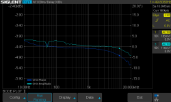
Bode plot showing frequency response:
Xc27ypo.png

Note that there's only -0.7dB difference between 10Hz and 20KHz. :D This is one side of the amp (ie one speaker terminal) running. With a differential input that's going to be at least +3dB.

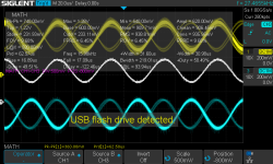
And finally - the upper and lower traces show each of the amps output and the middle shows the final output from the speaker simulated by subtracting the two:
LPBv25I.png

I have had some hiccups:
* blew two NPN transistors due to the collector rear pad shorting against the the grounded heatsink
* blew one fuse on power off (I've not fitted the MOVs yet to cope with voltage spikes caused by powering off the transformers)
* currently limited to 200mA due to the SOA of the NPNs as the LV supply with a 22Vac transformer is giving me ~32Vdc which is too high. This means I can only run the amp for a period as the NPNs start to thermally run away. Once I have the power down to 20-24Vdc I can run 600mA through before the SOA (safe operating area - ie approximately max power).

Todo:
* Toroid MOVs across the primary to stop the large voltage spike caused by turning off a large inductor (transformer) as the flux collapses.
* rectifier snubbers across the secondary - rectifier to remove the switch noise.
* Maida voltage regulators for each supply to reduce noise further - this will also reduce the LV voltage to 20-24V and reduce ripple at the same time.

Once that is done I'm hoping that the NPNs have enough cooling that I can run without a thermal runaway. If not then I have to fit a larger heat sink.

Next step I also want to add a balanced (differential) DAC. That will bring the system alive.
 
Last edited:
Your amp IS your power supply:

zecFvQn.png

The bottom left is the two amp channels.. the rest of the blocks are the regulated power supplies. Currently they're simulating in LTSpice but the small single model was showing a <1mA ripple on the 170V supply - about 16mV :D

N7OmrjU.png

With a 1V 1KHz signal input.. No 50/100Hz noise.. below 120dBV.. I suspect that will be rather quiet in real life too.
 
Last edited:
Ordered the components and a new bench power supply only to realise the bench power supply has a minimum current limit of 250mA. The only one I've ever seen that has such a stupid limit. Pity it's 60V, has 12V and 3.3/5V ports and is programmable using USB. However it can't limit under 250mA which is dumb. Instead I'll forgo the bells and whistles to have one 1-60Vdc and have a current limit that starts at 0V.

It's a SMPS supply deliberately to be small but it must be able to limit at low ish milliamps for testing components and stopping the regulator going bang.. once done the amp's regulated supplies can support very fine voltage control but they're not designed for robustness with shorts and current limit setting etc.

Never mind RMA and reorder..

The bench power supply will be useful for slowly testing different parts of the build and limit current draw before it causes component failure. I can then ramp up the voltages until I get to 60V and it behaves itself. Once it's ok then I can switch to the actual linear amp power supply. I can also use the bench supply with the scope to match the components better.

I've also added a VI Limiter to the NPN output transistors. The concept uses another transistor to monitor the current of the main transistor and if it starts approaching the level of current that starts causing overheating or runaway then it pulls down the base of the transistor thus throttling the output transistor. In a case of a short this would the limit the current of the output transistor and the amp power supply itself will limit too..
 
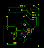
So I designed a 3080 regulator that will work for matrix board. That makes it easy to build and hand solder:
vYJQB0E.png

Currently I'm just testing ONLY the new power supplies and the 3080. The maida mosfet I'll complete and test tomorrow. Currently I'm sticking to low voltage. Tomorrow I'll solder in some more of the bits and bobs for the HV supply.

Zeq9f0v.jpg

ZPvBuoV.jpg

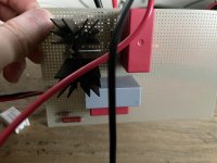
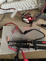
So I have the SMPS bench supply -> a LV RCRC taken from the amp -> 3080 regulator and then onto a 249R load.

I soldered in a 10V SMBJ, in fact that should be a 20V SMBJ as the regulator can cope with 37V, the LV should give the entire 20V to the 3080 and not get involved until it's over a 25-30V. So I should order a 25V SMBJ. That's the small surface mounted black square. For the HV supply this is less if an issue.

The 10V SMBJ gives about 11.6V before it opens up and conducts power. It's used as protection for the 3080 and can cope with 600W.

So for now I have - configured the PSU for 11V so the SMBJ doesn't conduct and measured what I'm getting.. peak-to-peak = 71mV.

lpIJZYt.png

No I'm not using ceramic output caps for the stability as stated In the datasheet, instead I'm using a metalled film cap (MKP4). I'm also not using a cap on the SET pin - I have one but it's one of the smaller surface mount components and that's too small for 200V use.
 
So after taking the regulator up to 25V I found a diode the wrong way around after I'd modified the board to cope with 200V without arcing over (1mm between the pads and removing those pads closer). With the mosfet installed I quickly got from 25V to 60Vdc. Then moved to the full 177Vdc of the amp rectrifier. The regulator is outputting 141Vdc at 26mA through a 5.5K resistor. So there's a little work todo as we're dropping 30V over the mosfet.

Looking at the mosfet gate pin - that's noise.. and output little noise.
RoNCGyn.png

This is better - I'm probing the mosfet output - you can see the residual ripple from the RCRC filter (about 200mVpp) the output is about 6.8mVpp if you ignore the very high frequency noise (RF and 1KHz spikes that are present when everything switched off so that's external noise coming through the mains):
iFMovdg.png

Checking the point that feeds the SET pin on the regulator - you can see the noise on the SET pin. I should add a small 10pF cap to decouple (allows the noise to bypass the regulator to the other side of the PSU):
zqiY7qz.png

So it's looking good - there's some points I will look at:
a) address losing 30V over the mosfet, it's sat a -4.5Vgs (ie gate to source) which means it's on the verge of switching off as the datasheet states 2.5-4.5Vg(th) at the point the chips start to turn on. So I may have to voltage double rather than play with the mosfet. Then I would have 245Vdc and use a resistor to drop to ~180V on the regulator output.

b) add decoupling caps to reduce the noise.
 
A small update. Work will slow down with the new job but there’s been some new things :)

First - two bench power supplies. Just cheapy switch mode 0-60V supplies which will supply 1.8A but these seem to be doing a good job with some limitations. These allow me to quickly setup dc power. One is a multicomp with aux power for 12v and 3.3/5V too. So i have effectively 4 power supplies supplies.
So far i’ve used them to test changing the LV voltage from 32V to 22V and the amp will run for hours without overheating. So i can use the LV regulator to drop the voltage once those are built.
I’ve also used then to power raspberry pis and a new gadget…

Second i have bought a 32bit 192khz AK5572 based ADC board for audio measurements and anaylsis. Whereas the scope is fast 200mhz and shallow with 8bit resolution, the 5572 is slower 32bit in thue at audio range with balanced inputs has a far higher dynamic range lower noise floor. The scope has a 40dB range offset by scaling whereas the ADC card has 130dB measured on a professional AP test analyser.
32bit, and even 24bit is a bit of a falacy in audio with most systems not getting above about 18bits aceoss a full system for various reasons however this card gives good performance for what i need.
The result will be high resolution FFTs and THD+N measurements. Essentially i get the performance of a £4K analyser for pennies with a bit of DIY work.

The adc board outputs i2s so my idea is to use the RPi zero 2w i have lying around to bridge between USB and i2s. This works and the mac simply sees the rpi as a usb ADC and DAC using standard usb audio - no coding required. I then attach the adc to the i2s on the zero.
For the 24Mhz clock iwill look at precision options but for now i can generate that using the PRI timers or using the hdmi output pixel clock (which if the right resolution, pixel depth and framerate is used will give a high resolution clock signal). The RPI will run headless and i may run a realtime OS/bare metal at a later date as there is a github project that does the same without having a large linux OS footprint.
The adc requires +15v -15v +5v so for now the bench supplies do a great job (smps will introduce some noise) i could even use the same LV power regulators for the amp to make the power even quieter with a small linear power supply. All things for the future. Getting it up and running in a case will be the first thing. I can worry about EMI beyond this at a later date.
I do have to be a little careful - the front end of the adc uses buffers and opamps to give a max input of ~3.6V. There’s no current protection so plugging an amp into the frond end would destroy it. The oscillopscope has 300V max front end so can test power supplies and low voltage tube amps.. for the headphone amp the scope can tell me the highest signal before i connect the ADC. I may make up some attenuators to reduce the voltage scaling 10x, 20x and 100x. If I use BNC. Connectors for the ADC rather than XLR I can possibly use standard BNC leads but i need to check the impact of 50ohm impedance.

I can then add a DAC for signal generation although current world silicon chip shortages mean those are in very short supply. Once we have one that can be added to the rpi.. An alternative is a signal generator but at £300+ thats blinking expensive but could drive around audio and clock signals. Perhaps an xmas present if the world has not imploded.
 
A small update since starting the new role which has slowed down the progress, on my plate for this:

On the amp:
a) order parts for rectification and regulators (I need to work out what values I need in light of some changes below)
b) switch from a full bridge rectifier to a voltage doubler - this means changing the bridge rectifier for a ladder of single diodes and capacitors for rectification that results in twice the input AC voltage. I can add more diodes and caps for additional doubling if required (I could get to ~900V by adding additional steps in the ladder but the current capacity drops by 1/2 each time). This is because the output from the regulators has dropped to 140Vdc so by switching I get to a higher input and can output 180V from the rectifier resulting in less tube distortion (the operating point of the amplification is at the intended 9-12mA idle current).
c) switch regulators from Schottky to zener as they're leaking current causing noise. Ideally for this purpose they should stay off until a problem causes them to conduct.
d) add a trim pot to allow the tubes current to be adjusted to balance to zero DC offset. I could do this automatically using a circuit board.

On the ADC:
a) order the parts for..
b) design a very low jitter 24.756Mhz master clock with a couple of outputs and possibly a clock divider for the i2S clocking. This is because the clock output of the RPI works but can only supply the max of 25Mhz with the frequency dividers. At this max the clock output waveform isn't good enough both in form (even if corrected with the Schmitt tigger) and that form jitters around the place making unsuitable for a measurement 32bit ADC.
c) design a very very low noise power supply for the master clock board - this will probably be a voltage reference and a BJT shunt. This can get crazy complex with temperature controlled ovens for stability but for me - a simple board at this stage will suffice.
d) design a clean +15V, -15V for the ADC frontend opamps and buffer, a squeeky clean +5V for the ADC itself (in addition to it's own regulators) plus a 5V digital supply for the RPI.
e) write the kernel driver for the RPI - I've done this already to the point it can be installed in the OS, now I need to complete it. I think the RPI's slow bus may be able to support 192K 32bit. I'd be using ALSA with a g_audio gadget to make the USB audio 2.0 sound interface (so you simply plug in the usb into the computer and it sees it as a capture device in any app). Then simply exiting ALSA to loop between the newly written driver and the g_audio.
f) finish the ADC configuration - that needs some additional component for AC only such as super low leakage capacitors.
g) design an attenuator box to protect the front end but allow sockets for 100Vpk and 400Vpk input BNCs channels to allow me to test higher voltages by using a simple voltage divider and capacitor - mimicking the oscilloscope probe. Currently the ADC frontend has a max of 4.096Vpp IIRC.
h) create a box - actually a box within a box to protect from EMI and lower the noise floor. Boxes of steel, copper cladded and mumetal are the eventual idea over time.

I have noticed that the ADC opamps get very hot - they're designed to run with ±35Vdc but they're running with ±17Vdc. In my book temperature is noise so until it's running I won't know if there's a problem or not. The odd thing is that the caps on the board also get hot - although I'm unsure if that's a switch on low ESR issue that my bench supplies will provide ~1.8A inrush. Or the PSU SMPS noise is causing that issue. Either way the ADC board draws its design ~70mA on each of the 15V rails.

So once the ADC is done - I can then use it to characterise the output of the amp such as THD+N and harmonics right down to about -123 to -127dB.
 
Given the issues with strikes and changing world craziness heading towards xmas.. I've just ordered myself a Silent SDG1032X signal generator for a combined birthday and xmas present. I can use this for both testing the amp with audio, stability with frequency sweeps outside of audio, AM/FM tuning, and clock generation for the ADC and later DSD stuff. In theory I should get it this week from Siglent UK.. not sure if the Mrs will take ownership of it for the time being. That 30Mhz model can be hacked to 60MHz in the same way the scope got software hacked from 100MHz to 200MHz.
I need to get some BNC cables but I'll order those with the next component batch. This also allows me to generate the 24.756Mhz clock for the ADC with a fair degree of precision until I have the thing running then I can worry about improving it with temperature controlled clocks and adding a DAC in the same package.
 
Last edited:
So I have the SDG1032X and just like the scope, the maximum frequency limit is controlled by a software key. In the old days this sig gen had to be hacked by playing at the linux level inside the unit but now it operates in the same way the SDS1104X-E does and the software key can be updated using MBCD through the SCPI interface.

The normal SDG1032X supports 30MHz max which is fine for everything except DSD512 (requires about 54MHz IIRC) and 768K samples/sec which requires 36MHz.. so a few minutes work and the sig gen is now capable of 60MHz which is the same as the SDG1064X. So happy with that.

I've also ordered the coax cables capable of 4GHz (BNC and SMB) for the clock, terminating 49.9R resistor (SMT), 50R terminators for the scope etc. The reason for the 50ohm termination is to stop RF signal reflections bouncing off the difference of impedance (it's like a difference in impedance (AC resistance) of material acts like a wall and reflects part of the signal back to the sender). The current cables aren't suitable for 24MHz so the square wave is very distorted and attenuated.

Once those bits arrive I should have a far better clock signal into the ADC, I can then set the system up for 50Ohm which helps improve signal transfer. I'll then use the bench supplies for the power (+15,-15,+5V) and the sign gen then provides the master clock signal. With the ADC set as master, the ADC will then generate the bit clock and frame clock for the ADC output from the master clock. Those additional clocks should then be clear on the scope.

I may have cooked the ADC chip at the weekend but if that is the case then a replacement is £10 for the chip. The pain will be desoldering the chip onto the board as it's a 48 pin surface mount chip!
 
Finally the RF cables arrived - I present to you a fully working deathstar *mwahahaha*

So this is the ADC. It's capable to 768KHz 32bit balanced with a decent noise floor.

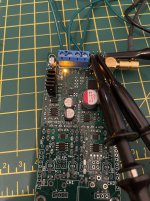
So the big square is a AKM 5572 ADC - capable of both PCM and i2S and here it's running at 192KHz/24bit but I will make it run at 32bit. The gold cable is a SMB RF connector which runs off to the signal generator acting as the clock. The blue block is for power connections, the black squares near the silver capacitors are voltage regulators and the two symmetrical sets of black blocks are the front end opamps - for bias and for differential input.

ba2iXnd.jpg

So to the proof of the pudding -

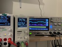
ntgeWpx.jpg

The two power supplies configured for plus and negative 14.75Vdc power rails, one supply has a great feature of a +12 and a +5V/3.3V power aux power which is perfect for this.
The scope shows a couple of traces - the bottom is the 24.576MHz clock that comes in over the SMB supplied by the signal generator, the blue shows the frame clock for PCM (basically the channel) and the middle purple shows and ever changing set of data bits - the digital output of the ADC.

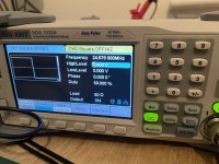
Next the SDG signal generator operating to create a clock sigal for the ADC:
PVpbdRK.jpg


The idea of this device is to make very good measurements of amplifiers.
 
Last edited:
So over the weekend I'll put in an order for some more bits.

This time it's a STM32 discovery board, case etc. The STM ARM chip will act like a USB audio device so you can connect the ADC as a high performance microphone in applications. The steel case will cut RF interference and keep all the components safe. Then I will write some STM code to transfer data between the ADC and the USB port.

For now, I'm keeping it simple and straight forward - I'll use my bench power supplies and the signal generator. To free those up, the next phase will see a quieter power supply and a higher precision internal clock.

I'll also order some components required to adjust the headphone amp LV power supplies to 22V. Plus a couple of other bits.

Then I can get myself back to testing the amp and sorting out the DC offset it has etc.
 
Back
Top Bottom