Nick's little project

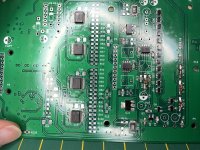
It's about time we had some more photos :D

1jLqIiE.jpg

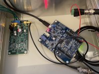
Board to the left - ADC board to the right STM32F23 discovery board.

I now have the STM appearing as a high speed USB Audio 2.0 device, capable of 192+KHz 32bit. Although in linux it seems happy the Mac seems to have issues at the moment.. so I use a RPI4 to act as the USB host :D

I've found my connection between the board isn't working well at the moment so I'm using a direct signal generator to create the signal for the STM's Serial Audio Interface (SAI) to lock onto (it's i2S/PCM) by using the signal generator channels to clock the bit clock and the frame clock (at 1/2 speed). This seems to work as I now get a interrupt and DMA for the SAI input:

tBZwN3v.png

Once this is working, the STM will act like a bridge so that the ADC card will appear like a USB Audio microphone :)


I've got the bits to make this and use the bench power supplies, including a scaling divider resistors so that it will take up to 400V peak to peak which will be useful for tube amps. I also bought a metal case so it will be shielded eventually.
 
Last edited:
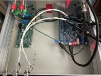
Ok, so I've neatened up the build, put some holes in and mounted some of the hardware - I'm also using the BNC connectors on the from for bringing in the clock signals for the STM whilst I develop the code. Once that's working I'll connect up the ADC (on the left) and away we go.
v6tJIJR.jpg
 
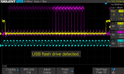
To explain what is happening - this is the output from the analogue to digital converter:
fmODJvj.png

The cyan blue trace is the SCK - essentially the bit clock. The yellow trace is the frame (or 'word') essentially indicating the difference between left and right channels - we're looking at one channel at the moment. The purple is the 24 bit sample captured in real time you can see the bits as the ADC outputs 24bit 192KHz.

This is the output from the ADC that is fed into the STM32F7 microcontroller on the blue card.

So the update today is - now the STM is interpreting the data from the ADC and storing into it's little 256Kbytes of memory in real time.

Previously I wrote a USB Audio 2.0 interface for the STM which appears like a microphone to a PC connected to it. The next step is to connect these two pieces of work so that the data from the ADC now in memory is returned by the USB Audio 2.0 request for streamed data.
 
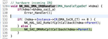
Well I found that the HAL firmware was hiding an error condition.. so after essentially writing the STM firmware for the SAI (ie the i2S interface) from scratch using direct register access.. I gave the ADC a long reset.. that's tweaking bits and bytes in memory locations.. and finally it freaking works:

PZAegVl.png

That's the DMA interrupt handler showing the hardware DMA double buffering working :D Now it *is* working :)
 
Been busy with work but had chance today to play with the code - I've started on the final software (the first was a couple of test projects that now need combining). It's now compiling and runs with the USB being seen but it's not entirely working yet. Still this is good progress.

The other thing I've done is designed a 24.576Mhz higher precision clock using a Crystek oscillator, a 1-3 fanout clock buffer (helps keep the integrity of the clock) with low noise power supplies. The fan out component is backordered until Feb next year, so it gives me time to sort out the PCB design. In short this should be better than my signal generator in both jitter (close in phase noise) and lower noise components in the ADC process should lower the noise floor further. The oscillator has a -170dB noise floor so that's well below my little signal generator and the ADC it self. The 1-3 fan out means I can then provide the same clock signal to three devices - the ADC, the DAC at a later stage and finally turn the BNC connector from an input to an output.

Lastly - back to the headphone amp :) - I will order the components for the voltage doubler (ie get to 180Vdc on the tubes), the replacement Schottky diodes for the regulators and a few other bits.

I'd figured a way to get a -1.5V power supply for the mosfet bias for balancing the amp ;) a Duracell battery or two in stack! The system will not use the power but it will use the voltage to maintain a negative rail. That way the VP p-channel mosfet that is there to help the auto balance of the system should work better :)

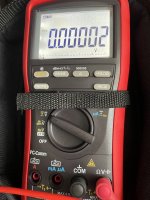
I also have a Brymen 869s multimeter coming to replace my decrepit no-name meters. It's CATIV 1kV and it still works after being given a 5kV shock (and did well against a 15kV test!). 5.5 digits and 50,000 or 500,000 count (ie higher precision) True RMS :) 1000V down to 0.01mV! It's about as accurate you can get in a DMM without going to a bench multimeter (those don't take well to abuse).
 
Last edited:
Better than the old meters by far! Quicker too. It also picked up the mains noise at 1.5Vac 50Hz :eek: how's how much noise having the extension cable on the desk gives!
mZ4mGzq.jpg

Was meant to be an xmas pressie but I got it early :D
 
Last edited:
So some progress - my USB Audio 2.0 class implementation is starting to be recognised:

Code:
pi@raspberrypi:~ $ arecord -L
null
    Discard all samples (playback) or generate zero samples (capture)
hw:CARD=STM32USBi2sBrid,DEV=0
    STM32USBi2sBridge, USB Audio
    Direct hardware device without any conversions
plughw:CARD=STM32USBi2sBrid,DEV=0
    STM32USBi2sBridge, USB Audio
    Hardware device with all software conversions
default:CARD=STM32USBi2sBrid
    STM32USBi2sBridge, USB Audio
    Default Audio Device
sysdefault:CARD=STM32USBi2sBrid
    STM32USBi2sBridge, USB Audio
    Default Audio Device
front:CARD=STM32USBi2sBrid,DEV=0
    STM32USBi2sBridge, USB Audio
    Front output / input
dsnoop:CARD=STM32USBi2sBrid,DEV=0
    STM32USBi2sBridge, USB Audio
    Direct sample snooping device

Awesome so the linux kernel and sound system (ALSA) now recognise it.

Code:
pi@raspberrypi:~ $ more /proc/asound/STM32USBi2sBrid/stream0 
Nick's DIY Audio STM32USBi2sBridge at usb-0000:01:00.0-1.1, high speed : USB Audio
Capture:
  Status: Stop
  Interface 1
    Altset 1
    Format: S32_LE
    Channels: 2
    Endpoint: 0x82 (2 IN) (SYNC)
    Rates: 192000 - 192000 (continuous)
    Data packet interval: 125 us
    Bits: 24
    Channel map: FL FR

And that shows it's being understood as a audio streaming device :D .. now I just have to fill in the audio streaming itself (ie write the data out when requested).
 
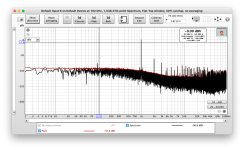
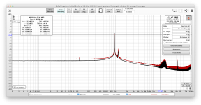
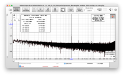
Vavva-boom! First FFT! Completely uncalibrated.

itfiG8Z.png

So this is going from a signal generator -> ADC -> STM -> Mac -> REW (the tool you see here).


Now calibrating using a single sided differential signal:

3GNx6iy.png
 
Last edited:
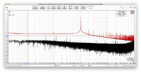
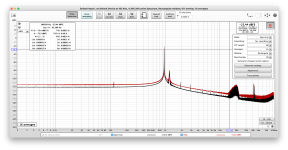
Ok, getting better- switching off some of the gear around it (the power supplies etc cause noise).

eT213TD.png

The red is my signal generator switched on... and the black is the sig gen channel switched off. Bigga-noise-droppa! In comparison, the 8bit scope FFT would give you around 40dBV dynamic range and so you'd not seen this.. so the effort shows it's worth it!

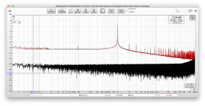
Fitting the metal lid also gives a decent indication of the expected performance:
AEEg0oF.png

-140dBV noise floor is spicy!
 
Last edited:
So I've been doing a little more internally, specifically adding a 10uF film coupling cap for each of the differential input lines. I've also sorted out some of the issues in terms of reference etc with the package I'm using (REW).

There's obviously a load of ripple noise coming in from the SMPS power supplies, enough to make a -100dBV spike at 50Hz plus a load of harmonics from the switching which (as it's a square wave, cause a mass of harmonics across the entire spectrum):
lq8vpzF.png

However that's good, it's consistent and can be removed by subtracting from the signal during calibration.

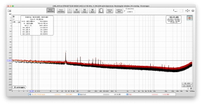
The next show the 14bit signal generator with a 2Vrms 1KHz signal single ended into one of the differential signal inputs.
iSuVKmE.png

First it shows how noisy and unclean the sine wave is! The noise floor increases by 30-40dB! Next the amount of harmonic spray from the digitally created signs wave is!
 
So what is next for the ADC..
1) a low close-in phase noise oscillator clock - currently the sign gen is providing the 24.576MHz clock, I want to make a small clock board which will provide 3 or 4 clock outputs. That will reduce the noise and jitter but the real reason for this is to free up the signal generator. SMT..

2) a low noise power supply for the ADC - this will then let me power the entire things off the mains rather than taking my bench power supply. The idea I have here will be be less noisy and use some high grade parts to provide a number of power supply rails. I have some ideas using LDOs and even voltage references to drive the LT3042s to very low noise (only issue is one of the voltage references is £14 just for a single chip, the LDOs themselves are £7 each at the moment!).
This will reduce the noise but also mean I can then use the power supplies for powering a DAC too.
I'd like to get that low noise floor much lower (specifically without 50Hz ripple) so I have a -120dB max for the noise floor. These will all be SMT..

What is apparent is that the signal generator (although very flexible) is noisy so I am thinking of making a very low noise analogue sine wave generator (probably 1KHz). However for now the sign gen works.

I also have a DSD DAC surface mount PCB I have to order, populate and finish. That will be very good but some of the components have long lead times so I need to get off my butt with the above to create a single order.

The same techniques I can use for the power supply for the headphone amp (I still need to finish that).

I tried stripping some SMT components off an old audio board but it appears that my 25W soldering iron simply can't sink enough heat into the large ground planes and the old board then simply disintegrates under the heat. It was a good test of both my bad skills and the reality check that I may need to get myself a better iron/hot air soldering station.
 
So I've been doing a lot of research reading around jitter (this may be interesting for others interested in DAC/CDP jitter): https://www.ieee.li/pdf/viewgraphs/jitter_basics_advanced.pdf

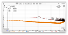
Looking at the above this appears to have _alot_ of noise:

* black line, the 1khz base is wide - this shows there's a lot of close in phase noise (ie think of this as jitter)
* the orange line (noise floor without signal) is high but the noise floor of the black line is even higher. This is because for every noise/harmonic/signal the phase noise base adds together thus the total noise floor in black rises.
* it appears the black noise up at 10KHz+ is due to periodic and interference noise on the clock signal and 1KHz signal.
* the orange line should be flat, however it's rising in the low frequencies - this is probably due to LF noise coupled with the master clock having phase noise (increasing the noise floor) but also 1/f noise from the noise power supply (you can see the 50Hz spike from the power supply). I suspect that the noise in the master clock is causing this low frequency increase. This mains ripple has harmonics such as 100Hz and this cares on into 200Hz, 300Hz etc for the harmonics..
* the high 40kHz-100kHz orange upturn is something called noise shaping - it's a technique used commonly in ADCs and DACs to shift the noise from the frequencies you're interested in (ie 1-20kHz) out of the audible range.

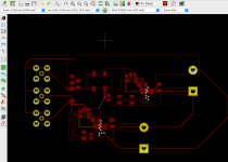
The clock I have planned is as Crystek CCHD oscillator with a Texas Instruments 1-3 fanout (ie 3 clock outputs). I have two LT3042s providing very low noise power regulation at 3.3V (input will be 5V):

D71nqEK.png

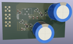
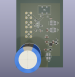
As a partial 3d model you can see what it will roughly look like:

YXOT9xX.png

Y1 is the crystal oscillator, IC3 is the fanout chip, U1 & U2 are LT3042 regulators.

I need to review this again with another PCB draft. The idea is good but I need to really make sure that the ground of the IC3 returns back to the lower LT3042 to prevent large ground loops. These components are *really* small being 1mm or below surface mount which should make soldering them to the board a challenge! (there's 0402 sized cap in there!). I need to add a pair of ferrite beads into this to reduce the noise further.

The thinking behind this is that the LT3042 needs a load to draw a decent amount of milliamps, so I may actually change the layout to power the entire thing with one LT3042 working harder (it can cope with 200mA max and the crystal is 24mA, the fan out IC3 chip is ~50mA max each so it's going to be close. This is why I may make it so that the power supply for IC3 can be shorted to use one LT3042 but have the option of populating the second LT3042 power supply.
Why all this power supply discussion?
The LT3042 and other "low drop out" (LDO) regulators have good noise rejection - in the order of 100dB which should help reduce the noise for the master clock crystal oscillator, which in turn will reduce the noise of the 1KHz signal for the analogue to digital conversion (in the same way a better clock makes a DAC better).

The fun with the LT3042 is that it's extremely sensitive, the SET pin needs the output voltage around it to prevent the SET pin from leaking current causing noise. The technique is called a guard ring. It essentially reduces the voltage difference and thus reduces loss through the PCB itself.

I have used the LT3080 (has the same sensitivity of the SET pin) earlier for the amp high voltage power supply. However the 3042 is even more sensitive and the resistors I am using for this are 0.1% tolerance. The surface mount capacitors are X7R which should provide decent temperature stability but they do suffer from piezo electric noise so if I make a mark 2 board I may need to use reduced noise.

I have the parts for making the PCB using photo resist and etching.. so this will be involved (next time around I may simply order the boards professionally manufactured from China).

TL;DR - new clock should reduce noise across the board but using titchy surface mount and making the PCB myself.
 
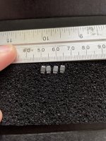
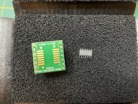
So the parts arrived.. this is the LT3042 I will hand solder..
7LCQEjv.jpg

:eek: :D **** me that's small!

However I also ordered a replacement op amp for the old A220. The 25yo (but still tuneful) MC33079P opamp which is still in production and is still respected as decent audio opamp (although old and is about 0.001% distortion). The replacement is a rather new burr brown audio opamp - the OPA1644A - which on paper outclasses the old opamp in just about every way. THD+N Distortion is 0.00005 % :D :D It's faster and slew rate outclasses too.

The outcome I hope is that the lower noise/distortion will increase clarity. The worry is that the amp may loose it's musical nature I like.. this is a good 2x magnified under the lens light.

T6nzd4S.jpg

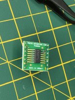
Some assembly required - I had to solder the DIP pins on the underside of the adaptor that is required to adapt the two chips. Thankfully the chips are pin compatible but the type of chip package is different.

That's cute. That's magnified too.. It comes in a sealed pack with a humidity paper indicator - if there's too much humidity absorbed then it will pop on soldering :eek: (it has a shelf life of 1 year in it's pack). My indicators were a nice blue.. but turned pink by the time I'd soldered it all together.

81YrDSE.jpg

The approach here is to clean the pads/pins with a flux pen then use a small amount of solder on a pin or two once aligned to tack the chip down. It's then a case to use a small amount of solder on each pin and the flux does the work.

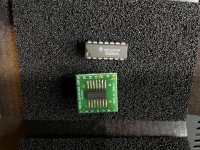
2dYPnV0.jpg

Old top and new bottom.

Only one issue - the pins of the old chip are thinner to fit into the DIP socket on the A220 main board. Doh! So out comes the 600 git wet/dry and then sand the pins down to size to fit the DIP socket :D Good thing it worked as look on Mouser, they are now out of stock!

So after a quick start up using a load resistor, I hooked up a pair of CHN50 nearfield speakers (small) to have a listen. The initial cold amp sounds harsh (this is normal with the A220) but hinted at some additional detail. Once the amp has spent an hour warming up (the output devices and VAS love to run at a hand scorching temperature as the amp is heavily Class A biased) the sound is both musical and exceptionally detailed. It's a keeper.
When I repaired the A220 I took the liberty in using some exceptionally low ESR (think they can charge/discharge fast) resulting in a preamp power supply operating at a juicy low 5 milliohms. This means solid and less noise/distortion for the new OPA1644A. It's very clear in very busy passages of music.

I will test on the Castle Harlechs at the weekend and I will do some additional measurements but for now.. it's a damn good upgrade.
 
Last edited:
So I've made a Mk2 design, this is better and takes into account some aspects - namely the 24MHz harmonics will mean designing for 250-500MHz, current loops, better grounding and layout. It also has a single 3042 with a set of ferrite chokes to filter - thus better noise rejection. As the total current draw is about 75-100mA I only need one regulator and it will have too little load (causes problems too).

P6EgdgN.png

This is what it should look like with some components in 3D:

MBsU5tj.png

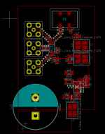
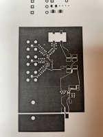
The size of the 3042 are minute.. Also I wanted to test the laser printer and if it could handle the design with 6 mil space used for making a coplanar strip line signal trace for the high frequency:

ZeaHq2d.jpg

Nope. So I will need to adjust the sizing that the laser printer is capable of. You may also just about make out a small area of circles bottom right - that's where I will need to solder the 3042.

I have an idea for creating a different design regulator using discrete components. Essentially in a later version I will replace the in-series regulator (3042) with a shunt regulator which is lower impedance. Only down side is it has less noise rejection over all but has a wider noise rejection across a wider frequency spectrum. All things that cause jitter.

So I think a 8 or 10 mil space will need to be used. That will change the properties so I may need to alter the design a little. However I'm feeling confident. Also I will need to drop from the 0.5mm via holes in the print above to 0.3mm drill holes :eek:

The idea is that I have an A4 sized double sided copper FR4 photo resist board. I will make a number of these with varying layouts so that if one fails to develop properly or has issues with the etch mask etc then I should have a usable board.
 
Last edited:
I've been busy at work but I've had a couple of designs suggested for low noise power regulation that you want for this.

There's two types of power supply regulators -
series - where the controlling device is in the path of current coming in. The regulator then uses that to control the current and maintain the voltage at the required level (ie 3.3Vdc at this case). The only down sides are higher impedance and noise (any device in the path adds noise).​
shunt - where the controlling device is acting like a controlled short circuit. This means the supply is at full current load and thus generates more heat but the regulator then diverts the unused current past the load device (ie the clock circuit) to maintain 3.3Vdc. The advantage is far lower noise as there's nothing in the path of the current from the power supply and that means it has a far lower impedance making it faster to provide power in dynamic demands for power. Downsides are heat and no current control if the regulator is shorted.​

The low noise 3042 and 3080 are both examples of series regulators, and very good (datasheet measurement of 2nV/sqrtHz noise). However I have two additional designs of shunt that provide less impedance and thus less distortion - one in the order of 20nV/sqrtHz noise (low frequency then dropping) and the other less dynamic capable but supposedly measured at 1.8nV/sqrtHz.

The issue with these noise figures is that they typically are for a specific frequency. Once you consider the wider frequencies and the power supply noise rejection (PSRR) over a frequency range and the purpose of the clock attached to the supply, those figures can be higher.
For example - the 3042 has over 120dB PSRR for the audio range.. that's really good for audio but it adds impedance to the supply so it's good with less dynamic changes. That PSSR number also then drops, so at 50KHz (outside of audio that number is far lower - allowing more noise through). Eventually at 100KHz the 3042's ability to regulate any noise out then runs out of steam and it's better to look at either changing the regulator or adding ferrite beads + caps are used to filter the higher frequency noise the 3042 can't cope with.

The second of the designs is a shunt and it has a voltage reference for low frequency (ie <20Hz) and a pair of 100MHz capable transistors then provide upper noise regulation but that runs out of steam at 1MHz. So ferrite beads with caps then provide filtering from 1MHz to 100MHz+. The beads I am using should provide 0.003 ohm impedance to DC current but that ramps up to 30ohms for 24MHz and then drops off more as it gets up to 100MHz. In reality I may need a further bead to provide 100MHz+ to 500MHz. The same will be true for the 3042's use of beads too.
My design has three sets of ferrite filters in series - the concept is that clock signal that causes power noise (ie the power demand goes up and down according to the clock signal being produced - essentially making a clock on the power supply as noise) and at each stage any 24MHz noise is then filtered and reduced. So by the time the noise gets back to the main power supply input it's had 90 ohms of impedance and been given plenty of chance to drop off to ground.. I hope that makes it quite quiet.

The third design uses non SMT components (old school!) but is supposedly better so I will try making that up as SMT (bending the legs to fit onto the board without holes through it).

The input for these will be 5Vdc, the output will be ~3.3Vdc and the max current draw will be about 100-200mA depending on the design.

I will then have three designs I've made for the PCB etching (large sheet so I can etch a number of designs and duplicates incase the etch fails). I will fit the power supply components and test the noise (as much as I can) using the signal generator to inject the clock signal to create noise on the power line (which the regulator can then combat). After that I can then look at the best option and build that supply with the oscillator (the decent close in noise 100dB oscillator I'm using are £27 each! and I've killed one already (oops), I found a even better -130dB oscillator is ~£160/each!).

And to that point about the dead oscillator - the max load is 15pF with 50 ohm load .. my passive oscilloscope is a 7pF+the probes and 1Mohm .. the result is large current draw and reflections back to the oscillator that destroyed it's front end (it's a small SMT component that has a circuit in it). I should have been using an active probe (£1K+) or an opamp to provide a low pF load and have a parallel load to bring the impedance to 50 ohm to prevent reflections. You live and learn.
 
Last edited:
So whilst waiting for the paint too dry (literally), I've been designing my power supply PCB - this is a design the PCB on a double sided clad board I have already so I'm limited in size to that. I'm hoping to use the laser printer toner transfer method.

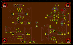
On this PCB (which will be rearranged - more in that later), is: top left - the -15V supply, bottom left - the +15V supply, bottom right - the +5V supply and the top right the +3.3V shunt supply for the digital isolator. The separate clock PCB will take it's 5V from this drive the clock and buffer using it's own 5V to 3.3V shunt.

7aZo5SH.png

Now this morning it occurred to me that the design should be flipped so that the 15V supplies are on the right. This is due to the 3080 pin out locations and I've changed the idea of using live heat sinks to grounded ones. I'll also reduce the impedance by making some of the tracks to be copper pours.

Interestingly, designing with surface mount components recently, the size of through hole components is frustrating! However these will dissipate the heat better and the reason for changing to the 3080 through hole instead of the surface mount 3080 is simply to allow for a heatsink. Cooler components means less Johnson noise (directly applies to value of resistance and temperature) overall. Less Johnson noise means less noise outright from the supply.

I now have two mouser deliveries - one for the power supply and clock etc and the other for a new project, both should be here next week.

Now to a new project entirely.. although it will use the power supply too. A Digital to Audio (DAC) :)

The next project that is bubbling away in the background is a MarcelvG Return-to-Zero DAC (RTZ). It's a DSD DAC only but capable of operating up to DSD512. Marcel designed this DAC after designing a tube version, and I have a set of PCBs after participating in a group buy.

I've also ordered the parts for this and 99% are titchy surface mount :D

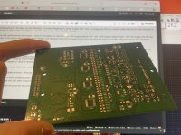
vhcTJ2u.jpg

There's more on the other side.. and another board too.

This DSD DAC will need some special work. Either you'd use a DSD streaming player or you'd use a PCM to DSD converter (typically in hardware using a FPGA). I'm wondering if the STM would be fast enough to convert PCM into DSD on the fly. The speed of the DSD512 bit rate is 54MHz IIRC, but DSD256 is near 24MHz so I could either use the STM internal clock out or a separate external clock (build a new clock PCB). The STM would then need software to convert the stream of audio from the USB connection to the DSD interface.
For now I can test the interface using my signal generator to generate a clock'd 1010...10101010 style 0V no signal to the DAC to test it.
Later I can use the same designs for the i2S digital isolator chips for the DAC. So although my work on the ADC is not directly related, the component designs for power supply, isolation and USB conversion can be used for it.
 
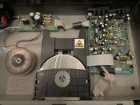
CD Player recapped last night as they CDP is 26+ years old and is starting to feel a little cranky:

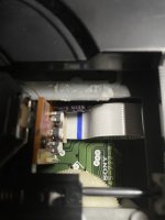
First this one that's buried in the CD player's laser assembly, photoed after I tested after and it worked.
XOSMF6h.jpg

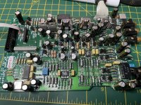
Next up is to replace every electrolytic cap (35 of them) on the main board:
qcFaVfQ.jpg

Previously this had Samsung SSL (220uF and 100uF) caps, with a few Rubicon Skyblues (100uF) for the opamp power supply and some 10uF 63V caps used for filtering. I changed these to 470uF, 180uF Panasonic FM caps and 150uF AZA hybrid organic caps but stuck with Panasonic 64V 10uF for the power filter caps. A slight bump for some of the caps for voltage (10V to 16V). Also as the CDP player runs hot and the output stage remains live whilst the CDP is on standby!, the caps are 105degC for longer life than the original 85degC.

I've changed the caps on the small power board previously.
KwOkqkA.jpg

vZoTcP2.jpg

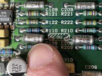
However it appears I hit one of the poly film caps in the process - this I believe is the root cause why one channel is currently dead (after investigating with DMM). They are soft so very delicate but also they're 1989 mil spec vintage.. so I've found some identical mil spec J160s (rather than F160) at the same 3.3nF that I've ordered. I'll test them with the signal gen and scope for a frequency response when they arrive.
However for now that cap can be removed (it will stop some filtering but that's going to be in the VHF range).

I also have the parts now for the ADC clock and power supply boards, the parts for the RTZ DAC should arrive today :)
 
It turned out that the cap was deader than a dead thing. It measures 0.011 ohms - a dead short which was dragging down the bias for the CD player opamp, the resulting output from the opamp sat at the -14V rail voltage. I have some 1200V 2.2nF FKP1 caps (yes a little over kill!) that fit precisely.. they support 11,000V/sec, so I think they'll do to replace these filter caps. So I thought what the hell and replace the cap with one of those.

So got ADC - let's burn a test signal CD, in this case a 1kHz tone and put the CDP on track repeat, and measure the output from the CD player.. (the repeat results in a spur to the right of the fundamental 1kHz tone)

Unaltered channel:
l0XBN0c.png

Now with the FKP1 replacement:

yxhrp6Z.png

There's a little improvement (the FFT drops), and he hideous noise shaping bump at the top of the audible range (15k-20kHz) in the noise floor however it's low enough for you not to hear it below -120dB.

The entire player seems to be happier with the recap:
a) the CD mechanism is more positive, seeks better
b) the front panel VFD display is almost back to brightness again
c) the sound seems good - although I'd not listen to A/B to hear a massive difference (may be the bass is better and some guitar picking/subtle effects seems clearer).
 
Last edited:
The good thing with the 1644A is its 100% pin compatible to the old MC33079P..

On the 1694 - it's not been released in the last 4 years, so I think that TI has given up on it. It's possible to make a adaptor with two 1692 but it's not a simple adaptor if you want to keep the low noise (ie a multi layer board).
 
So I decided to start the DAC soldering.. all hand soldered with an iron - no hot air workstations here!
HlHo3Ew.jpg

Just don't sneeze.

Some of the components are back ordered until November :( so the Idea is to finish this as much as I can so things don't get lost etc.
 
Last edited:
Back
Top Bottom