1st Gen HBM
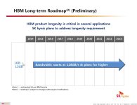
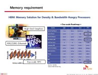
Hynix plans to put four DRAM slices over a single base layer. DRAM dies will be connected to each other with vertical channels called through-silicon vias (TSV). Each of those is capable of transmitting 1Gbps, which theoretically should give us 128GB/s of bandwidth. First generation of HBM would offer up to 4 dies per stack.
2nd Gen HBM
Hynix is still developing this technology. The company is currently testing 256 MB slices forming 1GB stacks. Soon, Hynix will start stacking 1GB dies to form 4GB modules. And we are just talking about 4-layer stacks. Nothing, except further research and development, is keeping us away from stacking 8 layers, only this option will only increase the capacity, as bandwidth will be limited to what 4-layers can offer (at least that’s what I’m getting from these slides). Second generation HBM will be available either 4 or 8 layers (forming 4GB or 8GB stacks). The speed per stack will double (256 GB/s).
http://videocardz.com/52874/hynix-high-bandwidth-memory-presentation-leaks-out
Please keep images to below 1280px wide or post in
tags like I've done for you above - Rilot


