• Competitor rules

    Please remember that any mention of competitors, hinting at competitors or offering to provide details of competitors will result in an account suspension. The full rules can be found under the 'Terms and Rules' link in the bottom right corner of your screen. Just don't mention competitors in any way, shape or form and you'll be OK.

AMD Radeon 300 Series Won’t Be A Rebrand, New GPUs Coming in June

It's as if people can't grasp something quite simple and fundamental. The way you get 4 or 8GB cards is by using double density memory, you can't design a gpu(sensibly) that can use 8 or 16 memory chips. IE one 290x that has 8 memory chips for 4GB and another with 16 chips for 8GB. The silicon itself needs to be designed with the number of connections.

Thus you can't just make a gpu that can use 4 or 8 stacks of HBM, it has to be designed up front for one or the other. Likewise the 4GB max is based on the concept that it will have only 4 stacks for engineering reasons and the supposed current maximum of 1GB per stack.

An AIB can't add 4 more stacks, likewise if there isn't both 1GB and 2GB stacks, AMD CAN'T offer two different capacity cards. I personally wouldn't want to pay significantly more for 8GB when I don't need it.

Not Often that I agree with DM, but I do agree with him here.

I also assume that unlike previous graphics cards the AIB's are not going to be able to change the configurations of the chips like they can at the moment.
What I mean is as it stands Gigabyte for example, gets the GPU from AMD, the Memory from Hynix, the PCB from PCB's R us, etc etc. They then assemble it all together how they want to and sell it to us, be it 4GB or 8GB.

Now a lot of the time the AIB's just go with the reference design as made by AMD (yes I know AMD get Foxconn or some other TW company to make it for them) but are they now going to have to have the get the GPU and Memory package as one component. Or, not that I can see it, they are going to be assembling the GPU die, interposer and HBM stacks themselves.
 
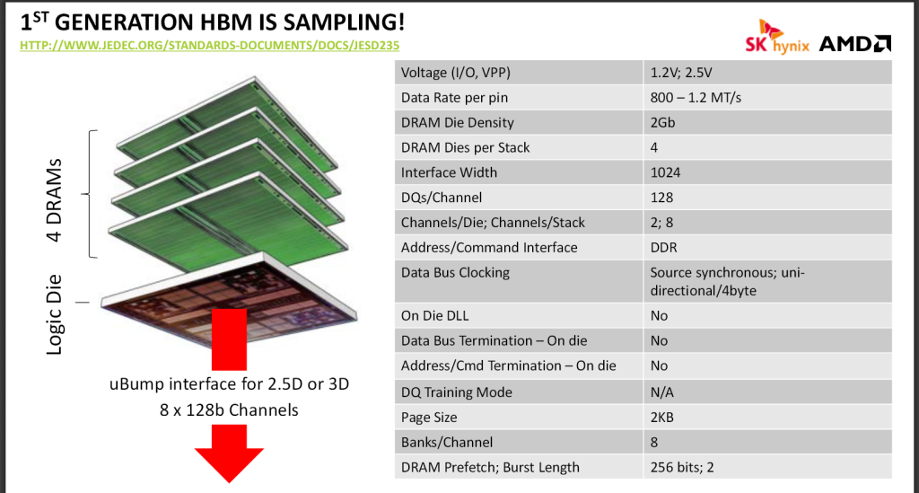
Fairly sure i read the SK Hynix presentation slides from 2014 or so that said 2gb per Stack for 1st Gen HBM, i might be mistaken but im pretty sure it was listed on the slides.

http://www.hotchips.org/wp-content/...Bandwidth-Kim-Hynix-Hot Chips HBM 2014 v7.pdf

On second glance you could be correct, although it states 2gb per DRAM Die, it also states 4 Hi Stack (1GB), so if that means your limited to 1GB per Dram on a stack of 4 equalling 4GB of Vram im not sure, although the 2nd Gen slide says 4-8gb versions possible.

However looking at this slide from AMD themselves

http://theconfab.com/wp-content/uploads/2014/confab_jun14_die_stacking_is_happening.pdf

you can see they clearly state - Dram Die Density 2GB, Dies per stack = 4, so hmmm not sure what to believe now

So it does.

According to that they should be 8GB.

 
2Gb * 4(stacks) = 8Gb (bit NOT byte) = 1GB
and as far as i know they can put 4 stacks on the interposer.
only 4GB for the first gen
 
Exxx; that's wrong might look up what Black Said from AMD back in 2012....interposer can be as large as they want; which means they don't have a limit on how much ram they can put on the card.

Their limit is end up by their interface which will most likely be 4096? for 4 GB; which will easily handle 8 GB....

Bryan Black, AMD’s head of the die stacking program gave a talk titled “Die Stacking and The System” in hotchips of 2012. In an answer to a question Black stated that engineers can use interposers of any size to meet their needs. They can be as large as 1600mm² or even 2000mm² to fit as many components as needed.

https://www.linkedin.com/pub/bryan-black/a/a8/b5

I'd believe him over just about anyone as he was one of the guys that helped develop HBM ;)
 
Edit ^^^^ ****** knows then...

So unless they find away to have two stacks on the First Gen or move straight to Second Gen its going to put people off.

More than 4GB is needed for 4K or Multiscreen, the viable option is people who want to drive 1440P at silly Frame Rates.
 
HBM.jpg


Hynix's own PDF which was linked to earlier, clearly shows 1st gen HBM being only 4 hi stack 1GB.

As for putting more than 4 stacks around the GPU on the same interposer, yes it is possible, but there was an article that was posted a month or so ago, that had a really good explanation as to why it wouldn't work for AMD to do that. Some thing about the bandwidth available and the pinout connections or something, I'll be dammed if I can find it though.
 
Last edited:
Exxx; that's wrong might look up what Black Said from AMD back in 2012....interposer can be as large as they want; which means they don't have a limit on how much ram they can put on the card.

Their limit is end up by their interface which will most likely be 4096? for 4 GB; which will easily handle 8 GB....

Bryan Black, AMD’s head of the die stacking program gave a talk titled “Die Stacking and The System” in hotchips of 2012. In an answer to a question Black stated that engineers can use interposers of any size to meet their needs. They can be as large as 1600mm² or even 2000mm² to fit as many components as needed.

https://www.linkedin.com/pub/bryan-black/a/a8/b5

I'd believe him over just about anyone as he was one of the guys that helped develop HBM ;)

First of all you're taking things out of context and not applying any sense to the numbers.

You can make ANY size gpu you want as well, you can just stick more than one die together, this is no different to interposers. Interposers are cheap and easy and they can be stuck together, hence to a degree any size is possible. But as above any size gpu is possible sticking them together.... that doesn't mean there aren't other limits, power(for adding more than one gpu die together), cost, yields which effect cost but also the general ability to put out a volume product. If you can get 2-3k wafers a month if yields are far too small then you simply have problems making enough to sell.

With interposers every chip you add you decrease yields, 4 chips is fairly easy on yields, only hurting yields marginally, more chips = decreasing yields because you can take lets say 8 good stacks costing maybe $10-20 a piece and a gpu costing maybe $100-200, put them on an interposer and one(of thousands) of connections fails and the whole lot, $300 worth, goes in the bin.

There IS a limit, it's smaller than you think. Being able to make a 2000mm^2 or more interposer doesn't mean you can fill it with as many chips as you want without any consequences. There will be situations where interposers are used to connect together several 500mm^2 dies in the future, which would still only be 4 chips being stuck down, not 8, or even more.

What is financially viable, what capacity of memory stacks are being made, how many stacks it's possible to make on a die are all unknown. However educated guesses say huge interposers are possible in the future but will remain used for applications where the costs aren't an issue, professional, server, super computer, semi custom, not volume lower priced chips.

As for their limit is the interface which is 4096, for 4GB, which can easily handle 8GB.... that sentence doesn't make sense. Each stack is 1GB and 1024bit wide, there are four connections and people are implying a 4096bit interface because of 4 stacks, you can't add four more stacks, that isn't how it works. It either has 4 connections to HBM or some other number of connections.
 
Hynix's own PDF which was linked to earlier, clearly shows 1st gen HBM being only 4 hi 1GB stacks.

As for putting more than 4 stacks around the GPU on the same interposer, yes it is possible, but there was an article that was posted a month or so ago, that had a really good explanation as to why it wouldn't work for AMD to do that. Some thing about the bandwidth available and the pinout connections or something, I'll be dammed if I can find it though.

The official specs are minimum specs and are there for two reasons. One, it's to help drive the industry forward, you can make X, now lets everyone try and make Y and all work towards those same goals.

The other one is really more naming than anything else. For one thing the 290x rumours have for a long time suggested a speed of 1.25Ghz, somehow no one goes "zomg, that isn't the spec, it's not possible", but if there was 2GB per stack people point at the spec as an all encompassing standard.

Look at any memory specification, do all sticks sold adhere to Jedec standards? Nope, never has, never will.

If you make a 2GB/1Ghz stack of HBM, because it doesn't meet HBM 2.0 specs(no 2Ghz) then it would only meet(and surpass) the HBM 1.0 spec, it doesn't mean it can't exist. Likewise 1GB/1.25Ghz wouldn't meet HBM 2 but would meet HBM 1. If and when we get 2GB per stack I don't know, it's fully possible and doesn't need to wait for the first HBM 2.0 chips to be possible.

We really don't know when increased spec HBM chips will be available. HBM has been sampled and in some level of production for 18+ months, the main reason it hasn't been used at this point is both cost and usability in lower capacity. There are always downsides to new tech, almost always cost but often other technical limits as production starts. The sooner we get a volume product with HBM, the quicker production will ramp up and the sooner we get to improvements in production which will be speeds, density, number of chips per stack.

It's absolutely not a given that 1GB/1Ghz is the only possibility, what we can say is 1GB/1Ghz is the minimum we know they can achieve.
 
Thing is AMD can look at this two ways, 1) Are we releasing something to compete with the 980? 2) are we releasing something to compete with the TitanX?

If 1) then they only need 4GB and to make the card faster by a decent amount and have better cooling than the 290X and they are on to a winner

If 2) then the card needs to have a minimum of 8GB of Vram, be considerably faster than the 980 and have a decent cooler to make it perform.

In all honesty we wont know anything about HBM and its performance until review samples are on tech sites being put through tests, until then everything is pure speculation unfortunately :(

Or 3) Neither of these, they're aiming to compete with the top end card that comes from the cut down Titan.
 
@drunkenmaster
do you have any idea on how will HBM do with heat?
i know it's small, has lower power consumption and the design has some holes so all of the memories chips in the stack get cooled, but i don't see how that heat transfer will work properly when you only actively cool the top one
also i believe the interposer will be taking part of the heat from the GPU

For higher power chips heat is a real issue for stacked chips, it's why we won't any time soon see on die stacking with anything like a gpu, just on package. Effectively it's look like 3-4W max per chip if you want 4 stacks, the 8 stacks might want that to drop further but there are some interesting heat transfer tricks.

Basically adding in 5-10% dummy TSV's effectively gives a copper connection that can just transfer heat from bottom to top dies. I can't find the graph now but it was along the lines of reducing the bottom chips temp from around 100C to 80C, with the top chip being around 70-75C in both cases. So a pretty healthy temp drop from something that is relatively simple to do.

HIgher power chips is going to be a huge no. Things like having a 20-250W gpu with memory stacked on top of it just isn't going to happen. The only places we'll see memory on top of a proper processor will be smart watches, places where size of the package is crucial. For GPU there is really no reason to stack on top of the gpu as there are no space issues to begin with but power issues mean it would be a non starter as is.

thank you for the answer.
so 10C difference from top to bottom chip is pretty good I would say. I was asking because of the OC potential and the possible heat problems / reliability of HBM.
 
First of all you're taking things out of context and not applying any sense to the numbers.

You can make ANY size gpu you want as well, you can just stick more than one die together, this is no different to interposers. Interposers are cheap and easy and they can be stuck together, hence to a degree any size is possible. But as above any size gpu is possible sticking them together.... that doesn't mean there aren't other limits, power(for adding more than one gpu die together), cost, yields which effect cost but also the general ability to put out a volume product. If you can get 2-3k wafers a month if yields are far too small then you simply have problems making enough to sell.

With interposers every chip you add you decrease yields, 4 chips is fairly easy on yields, only hurting yields marginally, more chips = decreasing yields because you can take lets say 8 good stacks costing maybe $10-20 a piece and a gpu costing maybe $100-200, put them on an interposer and one(of thousands) of connections fails and the whole lot, $300 worth, goes in the bin.

There IS a limit, it's smaller than you think. Being able to make a 2000mm^2 or more interposer doesn't mean you can fill it with as many chips as you want without any consequences. There will be situations where interposers are used to connect together several 500mm^2 dies in the future, which would still only be 4 chips being stuck down, not 8, or even more.

What is financially viable, what capacity of memory stacks are being made, how many stacks it's possible to make on a die are all unknown. However educated guesses say huge interposers are possible in the future but will remain used for applications where the costs aren't an issue, professional, server, super computer, semi custom, not volume lower priced chips.

As for their limit is the interface which is 4096, for 4GB, which can easily handle 8GB.... that sentence doesn't make sense. Each stack is 1GB and 1024bit wide, there are four connections and people are implying a 4096bit interface because of 4 stacks, you can't add four more stacks, that isn't how it works. It either has 4 connections to HBM or some other number of connections.

Come on DM now how long have you seen me post; not just here. I completely understand; I put that out there so others that keeps saying interposer can only be a certain size is wrong.

I very much think there will be 4 gig cards and 8 gig cards......but you are right about costs someone using 1200mm interposer the cost would kill it.......as you've pointed out with 1GB chips; that's just min spec...

things are going to get very interesting in next few months...
 
thank you for the answer.
so 10C difference from top to bottom chip is pretty good I would say. I was asking because of the OC potential and the possible heat problems / reliability of HBM.

2.5D HBM heat won't be a problem if you look at the white papers its perfect for high performance gpus. 3D is where heat can be a problem as its not connected to the chip by an interposer but is fully intergrated into the chip self and not just part of the package.......

3D is perfect for low power and embedded chips;
 
The problem is that AMD do not have the pull of Nvidia for what ever reason. So they need to price them competitive to make people move from Nvidia.

They never tried though AMD since the 3870 days have been all about value for money. If AMD made the fastest gpu on the planet enthusiasts will snap them up even if priced at Titan levels of rediculousness.
 
Back
Top Bottom