Soldato
Amazing Deal: 2000MHz Kingston Hyper X Triple Channel 3GB KIT

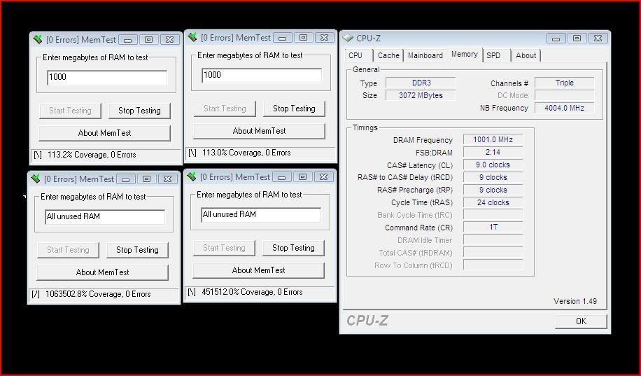
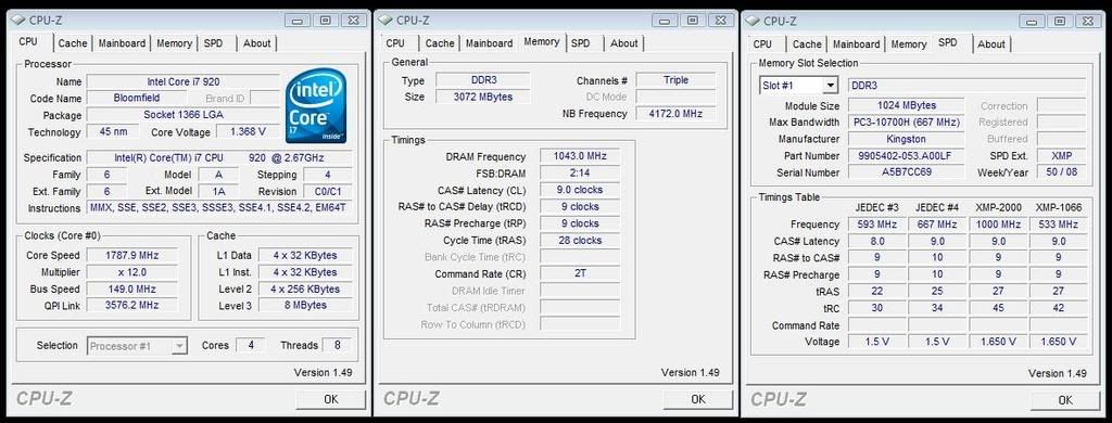
Kingston's KHX16000D3K3/3GX is a triple-channel kit of three 128M x 64-bit 1GB (1024MB) DDR3-2000 CL9 SDRAM (Synchronous DRAM) memory modules, based on eight 128M x 8-bit DDR3 FBGA components per module. Each module kit supports Intel® XMP (Extreme Memory Profiles). Each module kit has been tested to run at DDR3- 2000MHz at a latency timing of 9-9-9 at 1.65V. The SPDs are programmed to JEDEC standard latency DDR3-1333Mhz timing of 9-9-9 at 1.5V. Each 240-pin DIMM uses gold contact fingers and requires +1.5V. The JEDEC standard electrical and mechanical specifications are as follows:
- JEDEC standard 1.5V ± 0.075V Power Supply
- VDDQ = 1.5V ± 0.075V
- 667MHz fCK for 1333Mb/sec/pin
- 8 independent internal bank
- Programmable CAS Latency: 9-9-9-24
- Posted CAS
- Programmable Additive Latency: 0, CL - 2, or CL - 1 clock
- Programmable CAS Write Latency(CWL) = 9(DDR3-1333)
- 8-bit pre-fetch
- Burst Length: 8 (Interleave without any limit, sequential with starting address “000” only), 4 with tCCD = 4 which does not allow seamless read or write [either on the fly using A12 or MRS]
- Bi-directional Differential Data Strobe
- Internal(self) calibration : Internal self calibration through ZQ pin (RZQ : 240 ohm ± 1%)
- On Die Termination using ODT pin
- Average Refresh Period 7.8us at lower then TCASE 85°C, 3.9us at 85°C < TCASE . 95°C
- Asynchronous Reset
- PCB : Height 1.180” (30.00mm), single sided component
Buy Now @ Just £189.74 Including VAT
Kingston 'HyperX' 6GB (3 X 2GB) 'Intel® XMP' DDR3 2000MHz CL9 Triple Channel Kit

Kingston's KHX16000D6K3/6GX is a triple-channel kit of three 128M x 64-bit 1GB (1024MB) DDR3-2000 CL9 SDRAM (Synchronous DRAM) memory modules, based on eight 128M x 8-bit DDR3 FBGA components per module. Each module kit supports Intel® XMP (Extreme Memory Profiles). Each module kit has been tested to run at DDR3- 2000MHz at a latency timing of 8-9-9 at 1.65V. The SPDs are programmed to JEDEC standard latency DDR3-1333Mhz timing of 9-9-9 at 1.5V. Each 240-pin DIMM uses gold contact fingers and requires +1.5V. The JEDEC standard electrical and mechanical specifications are as follows:
- JEDEC standard 1.5V ± 0.075V Power Supply
- VDDQ = 1.5V ± 0.075V
- 667MHz fCK for 1333Mb/sec/pin
- 8 independent internal bank
- Programmable CAS Latency: 6,7,8,9
- Posted CAS
- Programmable Additive Latency: 0, CL - 2, or CL - 1 clock
- Programmable CAS Write Latency(CWL) = 9(DDR3-1333)
- 8-bit pre-fetch
- Burst Length: 8 (Interleave without any limit, sequential with starting address “000” only), 4 with tCCD = 4 which does not allow seamless read or write [either on the fly using A12 or MRS]
- Bi-directional Differential Data Strobe
- Internal(self) calibration : Internal self calibration through ZQ pin (RZQ : 240 ohm ± 1%)
- On Die Termination using ODT pin
- Average Refresh Period 7.8us at lower then TCASE 85°C, 3.9us at 85°C < TCASE . 95°C
- Asynchronous Reset
- PCB : Height 1.180” (30.00mm), single sided component
Buy Now @ Just £310.49 including VAT

Kingston's KHX16000D3K3/3GX is a triple-channel kit of three 128M x 64-bit 1GB (1024MB) DDR3-2000 CL9 SDRAM (Synchronous DRAM) memory modules, based on eight 128M x 8-bit DDR3 FBGA components per module. Each module kit supports Intel® XMP (Extreme Memory Profiles). Each module kit has been tested to run at DDR3- 2000MHz at a latency timing of 9-9-9 at 1.65V. The SPDs are programmed to JEDEC standard latency DDR3-1333Mhz timing of 9-9-9 at 1.5V. Each 240-pin DIMM uses gold contact fingers and requires +1.5V. The JEDEC standard electrical and mechanical specifications are as follows:
- JEDEC standard 1.5V ± 0.075V Power Supply
- VDDQ = 1.5V ± 0.075V
- 667MHz fCK for 1333Mb/sec/pin
- 8 independent internal bank
- Programmable CAS Latency: 9-9-9-24
- Posted CAS
- Programmable Additive Latency: 0, CL - 2, or CL - 1 clock
- Programmable CAS Write Latency(CWL) = 9(DDR3-1333)
- 8-bit pre-fetch
- Burst Length: 8 (Interleave without any limit, sequential with starting address “000” only), 4 with tCCD = 4 which does not allow seamless read or write [either on the fly using A12 or MRS]
- Bi-directional Differential Data Strobe
- Internal(self) calibration : Internal self calibration through ZQ pin (RZQ : 240 ohm ± 1%)
- On Die Termination using ODT pin
- Average Refresh Period 7.8us at lower then TCASE 85°C, 3.9us at 85°C < TCASE . 95°C
- Asynchronous Reset
- PCB : Height 1.180” (30.00mm), single sided component
Buy Now @ Just £189.74 Including VAT
Kingston 'HyperX' 6GB (3 X 2GB) 'Intel® XMP' DDR3 2000MHz CL9 Triple Channel Kit

Kingston's KHX16000D6K3/6GX is a triple-channel kit of three 128M x 64-bit 1GB (1024MB) DDR3-2000 CL9 SDRAM (Synchronous DRAM) memory modules, based on eight 128M x 8-bit DDR3 FBGA components per module. Each module kit supports Intel® XMP (Extreme Memory Profiles). Each module kit has been tested to run at DDR3- 2000MHz at a latency timing of 8-9-9 at 1.65V. The SPDs are programmed to JEDEC standard latency DDR3-1333Mhz timing of 9-9-9 at 1.5V. Each 240-pin DIMM uses gold contact fingers and requires +1.5V. The JEDEC standard electrical and mechanical specifications are as follows:
- JEDEC standard 1.5V ± 0.075V Power Supply
- VDDQ = 1.5V ± 0.075V
- 667MHz fCK for 1333Mb/sec/pin
- 8 independent internal bank
- Programmable CAS Latency: 6,7,8,9
- Posted CAS
- Programmable Additive Latency: 0, CL - 2, or CL - 1 clock
- Programmable CAS Write Latency(CWL) = 9(DDR3-1333)
- 8-bit pre-fetch
- Burst Length: 8 (Interleave without any limit, sequential with starting address “000” only), 4 with tCCD = 4 which does not allow seamless read or write [either on the fly using A12 or MRS]
- Bi-directional Differential Data Strobe
- Internal(self) calibration : Internal self calibration through ZQ pin (RZQ : 240 ohm ± 1%)
- On Die Termination using ODT pin
- Average Refresh Period 7.8us at lower then TCASE 85°C, 3.9us at 85°C < TCASE . 95°C
- Asynchronous Reset
- PCB : Height 1.180” (30.00mm), single sided component
Buy Now @ Just £310.49 including VAT


