Yes, but is it not fair to say that Fermi would have been better on 32nm, i.e, the wrong architecture for a 40nm process?
Also, is it not likely that Fermi on a 28nm process will be far more efficient and therefore profitable?
If you remember, it was AMD who did the re-spin with the 58xx series cards.
In reality, Nvidia would have been better holding off on Fermi until 28nm but it would appear that they were caught out by TMSC canning the 32nm process.
What we are seeing now is effectively Nvidia with the 5xx series & AMD with the 69xx series both with a full, efficient 40nm part and essentially now on a level playing field in terms of performance/efficiency etc.
I for one am really looking forward to 28nm and Q3 2011.
Let battle commence
")
No, 100% incorrect, theres ONE person i the world I see pushing this theory, his name is Rroff, Nvidia have not once claimed it, its known as a fanboy excuse.
At 32nm, "fermi" as we see it now, would NEVER have been 512sp's, ever, likewise 32nm was NOT schedualed, at any stage, for mid to late 2009, 32nm is due NOW, but was canceled, nothing more or less. This Fermi is all but the exact same chip as last years fermi, its a base layer respin.
A 6870 is NOT a base layer respin of a 5870, its a completely different design. You're talking about a 336mm2 5870, vs a 255mm2 6870, with a different front end, different dispatchers, but the same shaders, thats not a respin, at all, in any concievable way. A respin means sending the SAME design back with MINOR changes to tape out a second(or 3rd/4th/whoever many you want) times.
Theres is one single reason Fermi had problems at 40nm, architecture has nothing to do with process limitations, 530mm2 is a chip thats barely capable of being made on the process, its as simple as that, they decided to go with 512sp's, this is exactly in line with what we expected at 40nm, its NOT a 32nm design, anyone who tells you that is a complete idiot.
80nm 128shaders, 65nm 256shaders, Nvidia THEMSELVES dropped to 240shaders as 256 was too big to be made and 240was borderline and incredibly expensive with not great yields, 55nm was a optical shrink, AMD's 20% slower 4870 was still half the size just about as a 240shader 55nm version.
40nm should ALWAYS have been a 512shader design, always, the trend for a decade is a drop in process, a doubling of shaders in roughly the same die size area.
32nm would have been aiming at being a circa 700 shader part, in doing so, it would also have been 500mm2 + in size and would ALSO have manufacturing problems, because huge chips are a big problem as process's get smaller, every single other company that produces chips in the world knows this.
Yes, 32nm would improve yields and speeds of a 512sp Fermi, it would also improve yields and speeds of a 1600 shader 5870, so what, yields of essentially midrange parts aren't exactly a big deal and never have been.
AMD, 800 shaders 55nm, 1600 shaders 40nm. At 40nm Nvidia were always going to be bringing a circa 500 shader part, they did that, a year later they finally did a full base layer respin with very minor changes, at the same size that finally yielded a full part, anyone who suggests they were planning a similar shader 32nm high end part, is wrong.
AMD on the other hand are bringing a completely changed architecture, and its suggested their shader goal for 32nm was 2200-2400 or so, and they have indeed taken a 32nm design and moved it up while dropping some shaders/rops/tmu's to fit at 40nm.
Nvidia have done no such thing, Nvidia's plan was always to go for around 512 shaders on 40nm, this is obvious from the entire history of graphics and doubling shaders every full node drop, both companies have done this, for the best part of 20 years. This design schedual also put AMD at 1600 shaders for 40nm, no more, no less, they HAVE bought a design for next gen forward, Nvidia have respun an existing design.
First is first.
Shader structure, yes 6970 has new improved more efficient 4+1 structure.
This is a shader architecture improved NOT a GPU architecture improvement.
See the difference.
###
Next.
Yes your right there are shader improvements from one architecture to another. See above.
###
Third.
If you think improving shaders an adding more SD takes 2 years your on BADLY mistaken. Look at fermi as an example. Modified fermi 580GTX came out just 6months with improvements. Granted 580gtx it was a 480 with overclock and 1 core re-enabled but efficiency has still gone up by some 10%. You think that they were designing the 580gtx for 2years?
###
Lastly Fermi is a NEW architecture, hence it was late. Yes it has similarities with 8800GTX but they minor to say the least.
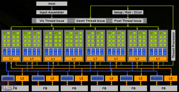
Anyway enough we the talk, pictures paint a million words.
Architecture is same and very linked. shader improvements, memory improvements, number of SD improvements.
Architecturally they are same.
Complete tosh, firstly, you're looking at top level architecture, and secondly, the 2900/6970 pictures look NOTHING alike, look at it carefully.
I think you're getting the same colours, and the same architecture confused here.
As for the 8800/Fermi, I said the SHADER's are pretty similar, since the 8800 the shaders are essentially very simple, basic shaders, one shader thats it. THe memory bus will be pretty similar, most of the core will be pretty similar, you are talking about arrangement of said pieces.
Moving a block of shaders here, to there, or increasing a shader block from 8 to 16 to 32, is incredibly easy but still takes a lot of time, changing from 8 of one type of shader to 8 of a complete other type of shader takes a lot MORE time. Nvidia hasn't really changed much with each individual shader sine the 8800, pictures DON'T tell a thousand words, those pictures are top level architecture, not a huge amount more than flow charts to give you an idea of how things change.
Every time you change the efficiency of the shader, EVERYTHING in the entire core needs to be tweaked to be balanced properly, look at the 5870 to 6870, balance of a highly complex shader structure is difficult to achieve. Which means, when you're waiting on the shaders all the time its hard to predict how many rops/tmu's/everything else you need and how to order and dispatch instructions efficiently.
Nvidia have a VERY simple shader structure, peak gflop throughout is rather the same as average throughput, its a one shader structure, its easy to predict and design the entire core knowing exactly hwo much performance you'll pull out. This is why Nvidia's architecture has had to change very little over time. AMD's is chaning a lot more dramatically on the uncore because peak and average throughput are no where near close to each other.
You're quite simply completely wrong. The 580gtx comes up as a gf100b in the bios when you flash it, Nvidia regard it(and anyone with half a brain) as a respin of gf100, a respin can take as little as 4 months, the "580gtx" chip SHOULD have been out Jan/feb this year, not next year.
When they got the first silicon back in JULY
2009, instead of doing a full base layer respin, the did 3 easier respins, which gained them very very little, its one or the other, not both. A non base layer respin only takes a couple months, they hoped it would work out, 4-5 months would have worked better than 2-3 times 2-3 months a piece.


 ) would say that wasn't very late to the party.


")