• Competitor rules

    Please remember that any mention of competitors, hinting at competitors or offering to provide details of competitors will result in an account suspension. The full rules can be found under the 'Terms and Rules' link in the bottom right corner of your screen. Just don't mention competitors in any way, shape or form and you'll be OK.

Intel kills 10nm ?? oO

Soldato
Joined
13 Jun 2009
Posts
6,847
Intel Xeon Roadmap Leaked Out, Unveils 10nm Ice Lake-SP With PCIe Gen 4 & Up To 26 Cores in 2020, Next-Gen Sapphire Rapids With PCIe Gen 5 & DDR5 in 2021

https://wccftech.com/intel-xeon-roadmap-leak-10nm-ice-lake-sp-2020-sapphire-rapids-sp-2021/

Good to see Ice Lake will have PCI Express 4.0 support to compete with Ryzen 3000 series but it seem PCI Express 4.0 will have shortest life in history compared to past standards and it will replace with PCI Express 5.0 12 months later. Look like a massive waste of time and money to implemented PCI Express 4.0 in CPUs, AMD and Intel should had skipped PCI Express 4.0 and straight to PCI Express 5.0 instead.
PCIe is always backwards compatible so it is not a waste of time in the slightest.

The roadmap is a bit strange. Why bother releasing both Cooper Lake SP (14nm) and Ice Lake SP (10nm) within 3 months of each other? Unless maybe they expect the Ice Lake parts to be at the lower end due to (Intel's admitted) lower performance compared to 14nm, or maybe they expect 10nm yields to be poor so need a 14nm chip at the same time to fill up the stack?
 
Soldato
Joined
26 Sep 2010
Posts
7,157
Location
Stoke-on-Trent
Of course! :mad:
So they still need to significantly crank up the bandwidth between the cores chiplet(s) and the I/O die.
Wonder what headroom they have with the current design?
That depends on how much headroom the current signal repeaters have on X570. Given PCIe 5 is "due" so soon after PCIe 4, it's possible AMD have factored this into the design of their PCH and board spec and over-engineered things so they only have some tweaks to make, rather than make it again.
 
Associate
Joined
27 Apr 2007
Posts
963
No. You can't even saturate the current PCIe 3 lanes, you can only dream of saturating double that with PCIe 4, and it's light years years away to even think about PCIe 5.
Just no.
The same chips are used in data centres where they are much more likely to be pushed hard bandwidth wise.
My point is that if you keep on doubling the external bandwidth at some point you have to increase the internal bandwidth or it will become the bottleneck.
 
Associate
Joined
27 Apr 2007
Posts
963
That depends on how much headroom the current signal repeaters have on X570. Given PCIe 5 is "due" so soon after PCIe 4, it's possible AMD have factored this into the design of their PCH and board spec and over-engineered things so they only have some tweaks to make, rather than make it again.
What about bandwidth internally between the chiplets and I/O die, does that need upgrading for PCIe 5?
 
Soldato
Joined
26 Sep 2010
Posts
7,157
Location
Stoke-on-Trent
What about bandwidth internally between the chiplets and I/O die, does that need upgrading for PCIe 5?
If I knew the answer to that I wouldn't be stuck coding stupid ad banners for an online betting company :p

I should imagine though there would need some level of parity to ensure the chiplets can deal with the information coming into the I/O die fast enough, but if such tweaks were needed for a PCIe 5-capable I/O die then AMD would update the Infinity Fabric accordingly.
 
Associate
Joined
27 Apr 2007
Posts
963
I should imagine though there would need some level of parity to ensure the chiplets can deal with the information coming into the I/O die fast enough, but if such tweaks were needed for a PCIe 5-capable I/O die then AMD would update the Infinity Fabric accordingly.
So they'd still need to update the core chiplets but presumably not as much as if they had to update it from PCIe 4 to 5.
Overall, there may be slightly more work than for the same update for a monolithic die, but a small effort for large gains.
 
Soldato
Joined
26 Sep 2010
Posts
7,157
Location
Stoke-on-Trent
So they'd still need to update the core chiplets but presumably not as much as if they had to update it from PCIe 4 to 5.
The chiplets themselves wouldn't need to change, but the signalling across the Infinity Fabric that connects chiplets and I/O die would need to be faster. Whether that extra speed requires better silicon for the IF remains to be seen, but AMD would know this and make changes accordingly.
 
Associate
Joined
27 Apr 2007
Posts
963
The chiplets themselves wouldn't need to change, but the signalling across the Infinity Fabric that connects chiplets and I/O die would need to be faster.
Is that an assumption unless you know the internal bandwidth that the chiplet can handle without needing updating?
If you keep on doubling the bandwidth going in to it at some point you have to increase the internal bandwidth otherwise it becomes a bottleneck.
 
Soldato
Joined
28 Sep 2014
Posts
3,437
Location
Scotland
PCIe is always backwards compatible

True!

so it is not a waste of time in the slightest.

Oh of course it a waste of time to developed chipsets with PCI Express 4.0 support! It took AMD and Intel about $300M to developed a chipset.

When PCI-SIG released PCI Express 3.1 spec back in November 2014, AMD and Intel did the right thing decided to skipped PCI Express 3.1 and decided to go straight away to PCI Express 4.0, in Intel old CPU roadmap showed Skylake to be the first CPU to feature PCI Express 4.0 support. AMD and Intel waited for PCI-SIG to released PCI Express 4.0 spec in 2014 and Intel planned to added PCI Express 4.0 in Skylake CPUs but PCI-SIG delayed PCI Express 4.0 further and Intel had no choice but to launched Skylake CPUs with old PCI Express 3.0 support in August 2015. PCI-SIG finally released PCI Express 4.0 spec in June 2017 while very busy developed PCI Express 5.0 but however both AMD and Intel decided not to added PCI Express 4.0 support in 2nd gen Zen and Coffee Lake then PCI-SIG released PCI Express 5.0 spec very quick in December 2018.

3rd gen Zen and Ice Lake should had PCI Express 5.0 in first place.
 
Soldato
Joined
28 Sep 2014
Posts
3,437
Location
Scotland
Last edited:
Soldato
Joined
26 Sep 2010
Posts
7,157
Location
Stoke-on-Trent
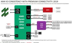
AMD Ryzen 3000 block diagrams leaked revealed PCI Express 4.0 is on chiplet die use for dGPU while PCI Express 4.0 on X570 chipset die use for slots, M.2 SSD, LAN, card reader and WIFI/BT.
That's the CPU, the chiplets themselves don't have any I/O capability, that's the point. So yes, the dGPU's PCIe 4 connection is handled by the CPU, it'll be the I/O die within the CPU that has the controller.
 
Soldato
Joined
28 Sep 2014
Posts
3,437
Location
Scotland
That's the CPU, the chiplets themselves don't have any I/O capability, that's the point. So yes, the dGPU's PCIe 4 connection is handled by the CPU, it'll be the I/O die within the CPU that has the controller.

You seemed confused with the CPU, chiplets and the I/O dies. The chiplets is the CPU dies.

When AMD unveiled CPU chiplets design approach back in November 2018, AMD showed the I/O die block diagram did not have PCI Express lanes but DDR and CPU chiplets controllers and said the CPU chiplets will have it own PCI Express lanes so the leak from Guru3D confirmed that CPU chiplets will have I/O capability.

https://www.anandtech.com/show/1356...n-approach-7nm-zen-2-cores-meets-14-nm-io-die

AMD’s chiplet design approach is an evolution of the company’s modular design it introduced with the original EPYC processors featuring its Zen microarchitecture. While the currently available processors use up to four Zen CPU modules, the upcoming EPYC chips will include multiple Zen 2 CPU modules (which AMD now calls ‘chiplets’) as well as an I/O die made using a mature 14 nm process technology. The I/O die will feature Infinity Fabrics to connect chiplets as well as eight DDR DRAM interfaces. Since the memory controller will now be located inside the I/O die, all CPU chiplets will have a more equal memory access latency than today’s CPU modules. Meanwhile, AMD does not list PCIe inside the I/O die, so each CPU chiplet will have its own PCIe lanes.
 
Associate
Joined
27 Apr 2007
Posts
963
Fair enough, I thought the PCIe controller was on the I/O die.
I did query you on that but you seemed so convinced and as I only have a passing interest I deferred to you.
But I did still wonder about the implications for latency and also internal bandwidth as if everything was passing between the two dies it might get congested.
Also, due to the size of the bloody thing (I/O die) I figured there must be more on there!
But at the same time, if the I/O die for EPYC has to host all the PCIe lanes for up to 8 chiplets then that suddenly seemed too much.
 
Soldato
Joined
26 Sep 2010
Posts
7,157
Location
Stoke-on-Trent
You seemed confused with the CPU, chiplets and the I/O dies. The chiplets is the CPU dies.
I did query you on that but you seemed so convinced and as I only have a passing interest I deferred to you.
No, I'm not confused, I know what a chiplet is, what an I/O die is and what a CPU is, and to be honest it still makes no sense for the PCIe controller to be on the chiplets. That quote from the Anandtech article is purely an assumption based on AMD not saying something (Tom's Hardware made a similar assumption), the article itself is dated November last year from a first look at EPYC Rome and even now AMD have not revealed information about the I/O die's full capabilities. And if the I/O die doesn't hold the PCIe controller too, why in the blue hell is it so big?

I've had a look around the tinterwebs and I can find nothing which states exactly where the PCIe controller resides in Zen 2. Plus, if the PCIe controller is on the chiplet, then that means CPUs with smaller chiplet counts will also have fewer PCIe lanes. So for example, EPYC Rome has 128 lanes available, so that's 16 lanes on each chiplet. X570 has 24 lanes, so that means there are 8 lanes explicitly blocked from being used? And does that mean ALL Ryzen 3000 CPUs will be dual chiplet implementation (and therefore using 4 lanes each to communicate with the I/O die) in order to get the 24 lanes? Because a single chiplet only has 16 lanes in it.

Furthermore, why would the chiplet in an EPYC Rome CPU be responsible for socket-to-socket communication? The whole point is I/O die to I/O die connectivity, lashing the 2P sockets together with 48 or 64 lanes, but the chiplet is responsible for that?

But at the same time, if the I/O die for EPYC has to host all the PCIe lanes for up to 8 chiplets then that suddenly seemed too much.
There is a Serve The Home article which talks about how EPYC Rome has a 8 sets of 16 lanes and how they can be configured to expose PCIe lanes for the system, lane allocation between sockets and I/O die to chiplet communication on the Infinity Fabric. That's 128 lanes available per EPYC Rome CPU. Only 128 lanes in an I/O die that size seems perfectly fine to me.


All in all, I'm not saying I'm right or wrong, I'm simply saying I don't know, nor does anybody else because AMD haven't revealed full details on the I/O die. But PCIe controller on the chiplet just makes no sense; the chiplets do the computing, the I/O die does the communication. That's the entire point, surely?
 
Soldato
Joined
18 Oct 2002
Posts
14,151
Location
West Midlands
The PCI-E controller for the EPYC layout is 100% on the I/O die, there is only IF links from each CPU to the I/O die. Not sure why people would think otherwise tbh, since even the layout of the Zen/Zen+ puts the CCX's behind the SDF and access to the UMC and I/O is in front of that. Now assuming that the chiplets are the same (99% certain they are) then the AM4/TR4 will have the same layout overall, with a shrunken I/O die for AM4 to fit the two CPU chiplet maximum requirement.
 
Soldato
Joined
26 Sep 2010
Posts
7,157
Location
Stoke-on-Trent
I was going to post that Wikichips page myself, but I didn't read down far enough to the Rome section to see it does state clearly what the deal is and therefore missed it. I blame my Friday pizza coma :p

The centralized I/O die incorporates eight Infinity Fabric links, 128 PCIe Gen 4 lanes, and eight DDR4 memory channels. The full capabilities of the I/O have not been disclosed yet. Attached to the I/O die are eight compute dies - each with eight Zen 2 core - for a total of 64 cores and 128 threads per chip.
 
Caporegime
Joined
18 Oct 2002
Posts
33,188
Also the I/O die is absolutely a chiplet, AMD just differentiated between the types of die with different names. The very concept of chiplets is in effect one monolithic die split up into multiple chiplets. Any chips that are required to add up to the whole are in effect chiplets.

Also Anandtech's take is incredibly poor there. AMD didn't list pci-e as being on the I/O die, therefore they are definitely on the CPU chiplets.... despite the image not listing pci-e there either. So Their take is if it's not listed on one chip it's 100% on the other chip. Thus you get stuck in an infinite loop, it's not on the i/o die, it's on the cpu chiplet. Wait it's not on the cpu chiplet it's on the i/o die, etc. The fact that the cpu chiplet lists no I/O while the I/O die lists... I/O as parts of the die, and you know it's called the "I/O" die, and pci-e is an.......memory interface, no wait, it's a processing core, no, a gpu, a bird, a plane, superman....... no it's a freaking I/O interface.
 
Back
Top Bottom