

Well i did say "an idea", comparing VII the product with any other product is relatively pointless, it's used as a basis because people wanted to get an idea of what to expect from the new fabrication process and based on Vega 56/64 specs we're probably looking at no more than a 15-20% increase in clockspeeds for roughly the same power draw.
-
Competitor rules
Please remember that any mention of competitors, hinting at competitors or offering to provide details of competitors will result in an account suspension. The full rules can be found under the 'Terms and Rules' link in the bottom right corner of your screen. Just don't mention competitors in any way, shape or form and you'll be OK.
You are using an out of date browser. It may not display this or other websites correctly.
You should upgrade or use an alternative browser.
You should upgrade or use an alternative browser.
Intel kills 10nm ?? oO
- Thread starter Zeed
- Start date
More options
Thread starter's postsBut as we discussed earlier, clock speeds don't mean anything in isolation. Hell, Vega 20 doesn't mean anything either. If Vega 20 was purely and simply a shrink of Vega 10 then we'd have a clearer idea, but Vega 20 was tweaked and added to as part of the 7nm work. The same power draw and only 15-20% clock bump could be influenced by there being more "stuff" to actually power and run, thereby skewing the numbers.
So yeah I get it's just "an idea" but I think there are too many variables at play for that "idea" to be sufficiently representative.
So yeah I get it's just "an idea" but I think there are too many variables at play for that "idea" to be sufficiently representative.
Not sure how you 'calculate' that. I.E. You didn't.
1) They probably won't shrink the design. 2) The shrink wouldn't be that large. 3) The shrink to TSMC 7nm probably wouldn't even be do-able without a major redesign. 4) Where are you getting huge performance uplift from? The 12nm node they're using is a bespoke SHP node designed specifically for NVIDIA and their large die GPUs. You might see frequency drops on the big chips. 7nm HP that AMD are using is certainly not SHP, and not a bespoke process designed purely for specific families of large die GPUs.
I would guess there'll be a new NVIDIA HPC card on TSMC 7nm+ HP in early 2020 (last month or so of this year at a push), then consumer 7nm+ stuff in Spring or Summer 2020. New architectures obviously, for both.
38% is the performance difference between TU102 and Vega 20, as of the techpowerup's benchmarks for 3840x2160.
If you add the normal, expected performance increase (clocks, mainly) going from 12nm to 7nm, which is ~20-25%, you get the result 50-60% difference between shrunk TU102 and Vega 20.
But as we discussed earlier, clock speeds don't mean anything in isolation. Hell, Vega 20 doesn't mean anything either. If Vega 20 was purely and simply a shrink of Vega 10 then we'd have a clearer idea, but Vega 20 was tweaked and added to as part of the 7nm work. The same power draw and only 15-20% clock bump could be influenced by there being more "stuff" to actually power and run, thereby skewing the numbers.
So yeah I get it's just "an idea" but I think there are too many variables at play for that "idea" to be sufficiently representative.
No, clockspeeds in isolation don't mean anything at the product level as different designs can effect performance, at the transistor level clock speeds are important, we're not comparing the performance of the products or different designs, we're comparing the performance of the transistors that go into making the product and like i said a transistor fabricated on the 7nm node switches around 15-20% faster than 14/12nm.
Well you didn't say transistor at firstand like i said a transistor fabricated on the 7nm node switches around 15-20% faster than 14/12nm.

OK, cool. Specificity is golden. Now where did you get that number from?
Well you didn't say transistor at first
OK, cool. Specificity is golden. Now where did you get that number from?
It can be even more:
"The initial 10nm process has 25% better performance or 0.56x better active power than the initial 14nm process."
https://www.semiwiki.com/forum/content/6713-14nm-16nm-10nm-7nm-what-we-know-now.html
"The 7nm process features SAQP for the FEOL, and double patterning for the BEOL. GlobalFoundries claims a 2.8 times density improvement compared to their 14nm process, and a performance improvement of 40% or a 55% reduction in power consumption."
https://en.wikichip.org/wiki/7_nm_lithography_process
Well you didn't say transistor at first
OK, cool. Specificity is golden. Now where did you get that number from?
Sorry, that's my mistake, i just assumed and made an you know what out of U and me, sorry about that.

")
The number came from how much higher VII on 7nm can clock than Vega 56/64 on 14/12nm (do they use 12 or 14, i can't remember), obviously it's not an exact number as we have to take account of density (the density will effect how hot the transistors get and ultimately how fast the can be clocked), 15-20% is basically my own personal best guess so you're welcome to make your own and we can talk about whose guess sounds more plausible.
It can be even more:
"The initial 10nm process has 25% better performance or 0.56x better active power than the initial 14nm process."
https://www.semiwiki.com/forum/content/6713-14nm-16nm-10nm-7nm-what-we-know-now.html
"The 7nm process features SAQP for the FEOL, and double patterning for the BEOL. GlobalFoundries claims a 2.8 times density improvement compared to their 14nm process, and a performance improvement of 40% or a 55% reduction in power consumption."
https://en.wikichip.org/wiki/7_nm_lithography_process
Comparing what Intel achieves, or across any other foundry for that matter, wouldn't really be comparable as the design of the transistor, design rules, steps, layers, etc, etc. Vary so much that one foundries 10nm could be another's 7nm. I'd also not put much faith in what foundries say the improvements are, I'm not saying they should be ignored, just that until what they fabricate is in a product that people can buy and test it's difficult to compare Xnm with Ynm, at least on a transistor performance level.
Last edited:
It's all good, my man, it's all good.Sorry, that's my mistake, i just assumed and made an you know what out of U and me, sorry about that.
I've just blown my abs out riding my fat ass up a steep hill so I'm perfectly happy to accept your numbers in the absence of my own cognitive ability! With applied context they seem logical. I do think though we'll see bigger improvements with Navi and Zen 2 given they're designed specifically for 7nm, not a shrink of a 14nm design, and nowhere near as complex as a Vega 20. Perhaps the 25% at the same power AMD used on their (revised) slides?
Ouch, IDK what blowing an ab is but anything to do with exercises is painful IMO so you have my sympathy.
Yea it could well be higher with Zen2 as AFAIK it's a fair bit less dense than a GPU so may be better at dissipating the heat, i just didn't want to over egg it and get shouted at.
Yea it could well be higher with Zen2 as AFAIK it's a fair bit less dense than a GPU so may be better at dissipating the heat, i just didn't want to over egg it and get shouted at.
38% is the performance difference between TU102 and Vega 20, as of the techpowerup's benchmarks for 3840x2160.
If you add the normal, expected performance increase (clocks, mainly) going from 12nm to 7nm, which is ~20-25%, you get the result 50-60% difference between shrunk TU102 and Vega 20.
You completely ignored what I said, and you certainly won't get those clock increases going from the 12nm process NVIDIA are using to the 7nm process that AMD are using. Nowhere near. You might well get an uplift going to 7nm EUV ... but that's speculative. We haven't seen any chips yet, and it'll be TSMC's first attempt at EUV. It could still be a bust. Indeed, one might say their hastily announced 6nm EUV might hint at performance issues which required non trivial design changes. Nominally speaking, it's very similar - in that it has only 1 more EUV layer (5nm has way more), and the optical shrink is minute. Why does it exist when 5nm EUV is scheduled for shortly after, if 7nm EUV performs as well as it should? I guess we'll see ...
Those TPU numbers were the very bottom of all relatively well known sites - as their AMD GPU results always tend to be, somehow. They're also from release.
I wasn't really paying attention and not sure if the information is public yet but there seems to be a low voltage, higher clockspeed but with some other compromise version they are doing - which probably hints that 7nm isn't hitting super high clockspeeds but it is still capable of a wide product range from low power to high performance.
Not sure how you 'calculate' that. I.E. You didn't.
1) They probably won't shrink the design. 2) The shrink wouldn't be that large. 3) The shrink to TSMC 7nm probably wouldn't even be do-able without a major redesign. 4) Where are you getting huge performance uplift from? The 12nm node they're using is a bespoke SHP node designed specifically for NVIDIA and their large die GPUs. You might see frequency drops on the big chips. 7nm HP that AMD are using is certainly not SHP, and not a bespoke process designed purely for specific families of large die GPUs.
I would guess there'll be a new NVIDIA HPC card on TSMC 7nm+ HP in early 2020 (last month or so of this year at a push), then consumer 7nm+ stuff in Spring or Summer 2020. New architectures obviously, for both.
You completely ignored what I said, and you certainly won't get those clock increases going from the 12nm process NVIDIA are using to the 7nm process that AMD are using. Nowhere near. You might well get an uplift going to 7nm EUV ... but that's speculative. We haven't seen any chips yet, and it'll be TSMC's first attempt at EUV. It could still be a bust. Indeed, one might say their hastily announced 6nm EUV might hint at performance issues which required non trivial design changes. Nominally speaking, it's very similar - in that it has only 1 more EUV layer (5nm has way more), and the optical shrink is minute. Why does it exist when 5nm EUV is scheduled for shortly after, if 7nm EUV performs as well as it should? I guess we'll see ...
Those TPU numbers were the very bottom of all relatively well known sites - as their AMD GPU results always tend to be, somehow. They're also from release.
I correctly ignored what you've said. Since you don't even mention that nvidia will probably use Samsung's 7nm process and not TSMC's.
Since you don't even mention that nvidia will probably use Samsung's 7nm process and not TSMC's.
I'm guessing its decided now but last I heard in terms of GPUs nVidia was still evaluating what process to use for their next gen GPU - also possible the Turing refresh is on a Samsung node but that might just be samples or something as part of the evaluation process.
I don't know if posted yet but extremely serious: https://www.pcgamesn.com/amd/amd-nvidia-7nm-graphics-card-performance
"Nvidia could drop 7nm GPUs tomorrow and AMD would be left in the dust
AMD will need to revolutionise its GPU architecture if it hopes to compete with Nvidia at 7nm
We’ve only heard light rumblings of Nvidia’s 7nm efforts so far, but the last rumours had Nvidia tapping Samsung’s EUV-enhanced 7nm process in 2020. The green team is reportedly a launch partner for Samsung’s upcoming process node, which, if all goes to plan, will offer performance gains not unlike those TSMC and AMD have brought to the table but on top of graphics cards that, almost effortlessly, outshine Radeon’s best efforts."
https://www.pcgamesn.com/nvidia/12nm-vs-amd-7nm-gpu-efficiency-incomparable
https://www.pcgamesn.com/nvidia/nvidia-7nm-euv-graphics-card-samsung
https://en.wikichip.org/wiki/7_nm_lithography_process
Associate
- Joined
- 27 Apr 2007
- Posts
- 966
Do Samsung have a recent history of producing high wattage and high performance silicon for CPUs or GPUs?
If they don't then that's doesn't mean their 7nm process won't offer that but I'm out of the loop so curious to know their recent history.
If they don't then that's doesn't mean their 7nm process won't offer that but I'm out of the loop so curious to know their recent history.
Do Samsung have a recent history of producing high wattage and high performance silicon for CPUs or GPUs?
If they don't then that's doesn't mean their 7nm process won't offer that but I'm out of the loop so curious to know their recent history.
They do all sorts though mobile/low power development has been more of a focus - their technology underpins Globalfoundries 14nm for instance which has been used for GPUs though seemingly GF was always 1-2 revisions behind Samsung's latest variant which hasn't produced the best of results for AMD.
Do Samsung have a recent history of producing high wattage and high performance silicon for CPUs or GPUs?
If they don't then that's doesn't mean their 7nm process won't offer that but I'm out of the loop so curious to know their recent history.
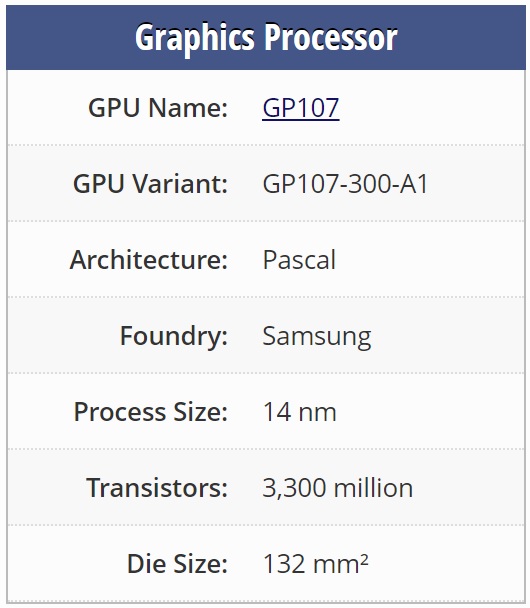
Samsung does it https://www.techpowerup.com/gpu-specs/geforce-gtx-1050.c2875
Associate
- Joined
- 9 Jan 2019
- Posts
- 885
I dont believe for one min that Nvidia could just "drop" a 7nm chip at a moments notice, if they could they surely would have already.
I'd forgotten about those Pascal GPUs that were produced on Samsung though they are towards the lower end power wise.
I dont believe for one min that Nvidia could just "drop" a 7nm chip at a moments notice, if they could they surely would have already.
It would be funny if nvidia pulls one 150 sq.mm chip that is as fast as the Vega 20
