Nick's little project

Ok, so I've been continuing to play :D

This is the current circuit - you'll note the front end being a differential amp, and from that point on - it's all phase split.
zDgDX8u.png

You'll note that it has a CCS on the front end (I2) - this works nicely, however trying the same on the second driver caused no end of issues so back to a cathode resistor (R9). Also I've disabled the DC servo as it seems to cause a problem that I need to get down to the bottom of. Anyway here's the output voltage and current (and the obvious DC offset):

js56ePH.png

Not bad into 32ohms. Just running a long 5 minute sim for an FFT.

27seconds of FFT after 30 secs of stabilisation:
NLpsnjq.png

Annoyingly everytime the screen saver kicks in the computation stops - doh!. Not bad noise base without any global feedback.

Edit: I found out why btw, the FFT is up to 1KHz - because I'd set 1ms as the max time step so the system will jump and accelerate when possible. Now I'm running the same at 20nS, the system is using ~670uS/S rate and it's been going since this morning ... it's modelled 12 seconds so far - so it's not even out of the 30 second stabilisation period (total 300 second simulation). A 300 second run will take 1,000,000/670 * 300 = 447,761 seconds.. or 5 days.
I need to work out how todo a faster calculation! It's running 12 threads on a 6core+HT 32GB Mac mini and only using about 18% CPU :/
 
Last edited:
Fixed the DC Servo and so the output is now -1mA offset which good enough at full amplitude.

However going with better resolution (50ns) has allowed me to trace back the source of noise.

Output from input stage (U2 in the schema) - the 1kHz tone and the small harmonics spikes:
YcKSXcp.png

Output from stage two (U4 in the schema) - lots of noise appearing, nasty amount of harmonics appearing:
H1Vy5Ca.png

And the culprit - both U3 and U4 are doing this. 1) the 14mA is way too high, and 2) the bottom of the wave form is clipping at 0mA
ZWxKqOS.png

But you wouldn't see that just looking at the voltage for each - it almost looks like a perfect sine wave:
LJTFYGl.png


Note that these FFTs are only 250mS from start (not like the 30s the posts above) and only about 2 seconds of run time, not 5 minutes. The noise seems to be lower overall but this explains the little bit higher noise atm.
 
Last edited:
The second stage (drivers U3 and U4) are soft clipping, however even when you play around with the grid and put 500V over it to give it plenty, you still get that clipping.. hmmm..

That section now has a I3 - a 12mA CCS running instead of the resistor. With the current over the resistor R3 & R4 also being in the order 6mA +/- 1.5mA or there abouts. So detaching the next output stage coupling caps (C3 & C4) just so that the driver tubes are running to the resistors R3 & R4 results in this:

PGtfLl3.png

An FFTing that wave form gives this (a few mS run so that's why it's an odd shape):

Wb5Ept7.png

Almost no noise - that's more like it! So the coupling caps that's causing the problem. In the run I have two 0.1uF caps in parallel - one feeding the 6AS7 grid and the other onto the output line itself (where it's cancelled out in part with the opposite phase.

This is looking very much like the issue:
https://www.aikenamps.com/index.php/what-is-blocking-distortion

The 0.1uF being too large can causing a problem.. let's see what a 0.022uF does :)
 
Last edited:
So I got the second stage working nicely.. only it outputs a very large peak - too large for the output 6AS7s.

Now if I cut out the middle stage - and simply go from the differential amp first stage straight to the output tubes- this is 1 second of simulation and FFT'd with 2M points:

N5wC1B9.png

Looking good so far. Just a second harmonic appearing :) this is natural as the amp is essentially running class A rather than class AB1 which will be the next stage.

I will connect the feedback and see if it needs that additional stage in there or not.

Just connected the feedback, probably will need an additional stage for enough gain to drive the output tubes to the right current & voltage... but this looks promising 300ms:

W4RCqcm.png

Just a hint of harmonics at the moment.

Edit update: And indeed after 2.3s the second harmonic peak is tiny (<10dB) vs the current sub 80dB floor.
 
Last edited:
Also for your viewing pleasure.. a DSD512 implementation of a ValveDAC using three 6SN7 valves per channel. No DAC chip.. just sigma-delta DAC implemented in valves.

xpRFkXW.png

The idea is this could be a 'front end' to driving the 6AS7 - direct DAC to headphones :D
 
Ok there were some serious issues with the LTSpice modelling of the 74HC chip (it's a digital chip that runs 0-5V but we're running at -137 (0V) to -132 (5V) relative. So after some (a lot) messing around...

Here is the ValveDAC output on start up
fZPOuKy.png

At 130uS the left chip voltages cause a first trip, then at 300uS the other chip finally gets down to -137 (this is due to the coupling capacitors). Then the system is just running 01010101010101... DSD 512 bitstream which gives a differential output (both present in the plot) that should = 0V when combined.

Not bad - 100+ year old tech running DSD512 :D DSD512 is 512 times the sample rate of a CD.

Now to the fun bit - if I switch out the e88cc valves to 6SN7s and tweak then this can directly drive the 6as7 output tubes into my headphones (32ohm) or direct into high impedance headphones!
 
Last edited:
So I will say nothing is 'new' and the designs and ideas are probably about there but I've been on a bit of a journey to understand the technology (tubes) understand the designs and the tools.

My guiding principles are:
* Low noise
* Tube stages - with a little help from solid state if needed.
* Headphones - capable of 32ohms
* Class A / AB1
* 6SN7 and 6AS7 based

Design topologies I've experiemented at in my earlier stages:
* SE 6SN7 -> 6AS7
* 6SN7 phase split using concertina -> 6AS7 PP
* 6SN7 input -> 6SN7 LTP -> 6AS7 PP
* 6SN7 other variants of 6SN7 drivers, differential amps, etc
* Negative feedback
* 6SL7 ..
* A 6SN7 version of Marcel's Valve DAC - including driving 6AS7 PP...

So from a LTSpice perspective I feed comfortable with the 6SN7 and 6AS7 and 'ideally' getting what I want...

So with the last piece it's got me thinking of the first stage - and how could I combine common components for the Valve DAC (requires six 6SN7 for both channels).

Then last night I thought - ignore everything you have done, focus on point 1 - noise. After reading around.. focusing on low noise designs for tube amps, removal of caps, reduction of resistors, paralleled tubes, differentials, and ensuring the majority of gain happens in one stage. Some of the ideas I was thinking about:
* Max 3 6SN7s - a total of 6 triodes available
* reduce resistors, capacitors in path
* Earliest gain possible
* Parallel - increase SNR
* Differential - reducing common noise
* Cascode - increasing gain without needing a coupling cap

I found a different back end stage - balanced but given the topology and the use of non-balanced headphones I would prefer PP with an output cap plus crowbar for safety.

So this morning I have decided on this topology:
ahRBmc5.png

The volume control is phase based. As a differential amplifier amplifies the difference and rejects the common signals, by varying the scale of the difference, it's possible to (a) control the volume (b) present noise on both channels (which results in noise been cancelled in the output stage) and (c) sticking with best practice of not putting a variable resistor ahead of the input stage.

I've just done the first run with some guesstimate non calculated cap and resistor values - even the bias on the tubes is not correct at the moment. However it looks promising:
xw4QfeN.png

So I think I will continue down the path of this topology as it's looking promising without correct values or negative feedback.

Just trying a feedback version - it takes a good 30 seconds for the system to stabilise but a 5 minute run should give an idea of the frequency spectrum.
 
For kicks just connected the feedback and ran it for a 5 min run (still not updated the values so this is like random values at the moment) - this is a slice after stabilisation with the negative feedback.. I thought - god that's awful! The I noted the scale on the side.. I'm starting to like this topology..

uBeM46g.png
 
So I had a bit of brainwave last night at 4am.. so I had to get up and try it. Instead of using a bypass resistor to increase the current in the front stage, I've added another 6SN7 as a second cascode but this time providing output to the alternative phase. This means noise from one side is then present on both channels - which is what you want. The differential amp of the push pull then cancels out the noise and you get the difference between the two signals.. Also increased the B+ to 600V to give the cascode stacks more headroom and allow a higher value Ra to increase the peak-to-peak output.

DA6RcqB.png

This is without negative feedback and class A.

I made a change after starting the simulation (set to maximum accuracy at the expense of speed) so the cascode grids are tied in the simulation but not in the diagram.

eviZfXr.png

U4 (signal) & U1 are a differential pair in a parallel formation with U5 & U2.
* Parallelled increases the signal to noise ratio, so less noise.
* this is a differential input stage and can be switched to take a balanced input from source, or, a single ended input as defined here. It outputs a differential - so it's the difference between the two outputs that is amplified, common signals such as the same noise are then cancelled out.

U6 is a cascode for U4 & U5, it increases the bandwidth but reduces the gain and peak to peak output, U10 is the 'anti'-cascode for U4 & U5 it's role is to pull current but instead of add signal, it's to provide the anti-phase signal and the noise from U4 & U5 etc to the anti-phase channel (U1... U7).

The front end is mirrored U1,U2,U3,U9, doing the same - except it's noise is copied across to the in-phase channel.

U7 and U8 are the output stage - as a push pull they will cancel out any common signals such as the same noise, and amplify the difference between the two phase channels as the output.

Volume control (R11, R12) works by allowing the phases to cancel each other out reduce the amplitude. It's current set to max volume.
 
I've been tuning quite a bit:
* Stacks are running +300 to -300 rather than 0-600V. There's an option to here to 'fold' the stack and have it all running nicely in less voltage but I'm saving that till later.
* Coscode stack now runs it's bias via a fixed voltage divider
* CCS on both stacks - set to 18mA so 9mA through each 6SN7.
* 6AS7s are now running a fixed bias but setup so that the resistances that the couple caps are identical, only issue is C2 needs 1.1KV through the resistor! There's got to be a better way to bias than have it with different resistances.
* removed the cross connects in the front end between the phases.

Result is this at 1KHz and 10KHz based on a 1 second run (so this is still settling after power up):
LkBDtST.png 6GqgiMq.png

So considering you're not going to hear anything under ~100dB.. that's a pretty quiet non-negative feedback! It's got Class A tube harmonics too.

I still have some additional work - looking at the frequency response etc.

Just running a 60 second sim. Typically these are GB of info so and they take their time for the longer runs.
 
Last edited:
So there's some optimisations and perhaps 'simplifications' to the design needed, one such change is 'folding' the cascode. Essentially this means (a) you keep the benefits and (b) you reduce the voltages required (they're needed to provide headspace for each valve in the stack) to something a little more reasonable - that alone allows you to have a wider range of components to select from - instead of +300.0.-300 configuration (600V rail to rail!) this could, in theory, be dropped to +120.0.-120 (240V) for example. This also reduces heat, plus if the folding is performed by solid state (JFET or MOSFET) it allows the number of tubes to be reduced (again reducing the heater power & power requirements). The solid state can also be configured to have enough driving power for the 6AS7 output tubes with ease.
As the backend 6AS7s run at 120V, the power supply will most likely be a 250V split +120.0.-120 and some space for inefficiencies. Just using solid state, means two tubes are dropped saving a total (both channels) of 0.6*6.3*4 = 16W saving on the heater power supply, allowing a smaller PSU to be used.
This also reduces the real estate required for the amp (both channels) means 4 less tubes (6SN7 isn't particularly miniature).

I'm leaning towards JFETs at the moment, as these offer a flatter response curve. For safety, they will still need to support the voltage across the rails - a 5V part isn't going to work here!
 
I've started on the simplification of the amp - currently it only has 0-320V (and 120V) power rather than the ±320 rails (ie 1/2 the voltage). I may up the power to 400V so the tubes have little more room. I've removed the upper set of tubes (this saves 2 tubes per channel) and currently use PNP transistors to reduce the cascode.

hO2fWEX.png

Starting to now focus on tuning this format, then I can design a power supply.
 
Working to reduce the power requirements further - this 'folding' allows you to implement constant current 'sink' (I1 & I2) and a constant current 'load' to replace the resistors (R6,R19,R25 and the mirrors). The only difference is that the output of the 6SN7 is current rather than voltage, this then uses the Q5 to drive R29 to create a voltage swing.

MJUsHx7.png

So this looks like it will work with 200V - thus should run off a 230V secondary. I still need some experienced feedback on this 'hybrid' design but the sim is looking ok.
 
So I've been researching more.

1. I've switched to e88cc valves on the front end, these take less B+ voltage (two in cascode only need 400V rather than 600+V) AND more importantly, this offers easier headroom in a hybrid cascode. Lastly the heaters are less current too - bonus.

2. I've gone down to the maths, so now I have a better understanding of the PNP (ZTX588) to tune it. I now have 100V peak-to-peak swing going into the 6AS7s, this is enough for the 32ohm headphones as I get 4V-peak and 140mA. So there's some room to adjust. Also a more accurate term of this topology is a shunted cascode rather than a folded cascode.
To perform the same in valve land I would need e88cc valves for the upper valves of the cascode, and then a separate differential driver section paralleled (overboard but averages the noise thus keeps the SNR focus).

So for stereo the difference between using a PNP and keeping tubed:
PNP: 4x e88cc tubes (200V) + 2x 6AS7 tubes (120V)
Valves: 8x e88cc tubes (400V) + 4x6SN7 driver tubes (320V) + 2x 6AS7 tubes (120V)

Now the idea all along is to have a headphone amp that is both a DAC and an amplifier for analogue line-in.

Marcel G's original ValveDAC used three e88cc valves per channel with a butterworth filter that re-constructed the analogue (the benefit of DSD is it's easy to reproduce analogue). When you look at the topology it is very similar to a cascode, but the input signals are different and there's an interconnection differences top and bottom. The signal is a 5-20MHz digital on/off and a 27Mhz clock signal - again digital on/off.

3S85rEs.jpg

So this leads me to a few options (valves are quoted for stereo):
a) Have a separate (400V) 6 tube DAC converting DSD to line level and then the amplifier - either 10x e88cc+2x6as7 or 12xe88cc+4x6SN7+2x6as7s.
b) Combine the analogue and amplifier - make the 6 tubes 8 tubes, keep at 400V, then simply switch connections to switch between digital DAC amplification or analogue amplification using the same tubes. The PNP, now acting as a driver, will be at it's max being a 400V part but when you look at the design by shifting the tubes to be -400V to ground, the voltage at the top tubes is actually very low - around 100V which the ZTX558 are comfortable doing on a continuous basis. This would be 10 valves (8 e8cc and two 6AS7s).
c) Combine the two as for (b) but remove the upper tubes and using the PNP to it's fullest. Issue here for purists is that the DSD signal is normally fed into the top valves, but if I use this method this would be only the clock signal being valved, the DSD signal would have to be solid-state switching. The benefit is I still stick to 200V and only the smaller 4xe88cc+2x6AS7s.
 
Looking at a solid state output rather than 6AS7s, I'm exploring this at the moment (just put in):

n1cjSdx.png

This has a common gate then a super follower as a voltage buffer - this presents a high impedance to the tubes and common gate (keeps the voltage swing) and then presents a low impedance to the headphones. The SF gain is less than 1 (same as 6AS7s) but is putting out about 400mA atm.

I'm attempting to get into the 0.0x-0.00x output impedance. Which is as good as a Chord Mojo..
 
An update - I've decided to keep it simple but able to be enhanced over time.

The original Broksie design uses 12au7 and three ecc99 tubes. The input signal is amplified by the first 12au7 triode, the signal travels through the cathode into the second 12au7 - no amplification occurs except the signal feedback from the output is used to reduce noise/distortion. The signal then runs into the paralleled ecc99s. The DC is then blocked by C2&C3 and then the signal then goes out to headphones R19.
I've enhanced the design slightly, adding noise cancelling by channeling noise through the CCS (constant current source) M1 & M2, these act to limit the maximum current but also flatten the load line horizontally so it doesn't change slope and cause additional distortion.

2UIusPX.png

Exploring and simulating the circuit shows it's very good, but only when it's operating at the average 447mV peak of consumer line-in, as soon as you put 3.16V peak in (this is the recommended 20dbV headroom to cope with transients such as cymbols or electronica etc) the amount of harmonics increases heavily. Additionally and more importantly, over 1V peak input caused the output DC offset to increase giving +6V to -2V peak to peak, so something that headphones aren't going to like on a continuous basis.

447mV at 10KHz
Xo7oATO.png

3.16V at 10Khz
lFQlYqu.png

So tracing this offset issue comes back to the input section (12au7) is outputting a larger positive sine wave lobe - this is down to the tube load line and this asymmetric distortion is also the cause of the increased even harmonics.
The 12au7 isn't a particularly powerful driver tube - so typically it's operating with in the form 12au7->12ax7 to offload the driving of the next stage to the 12ax7.

I've considered switching the 12au7 to a 6sn7 which is the older version of the 12au7 and is more able to drive, has less noise, and is more linear but it's also considered to be a little more bassy/boomy. The 6sn7 improves the situation, but complicates the power requirements (320V).

3.16V 10Khz 6SN7 replacement (I'm more familiar with the 6SN7 hence my initial guess at operating it is better):
MFbouHB.png

A suggestion for a more linear and less distortion is the 12bh7 which runs at 12V and 150V too.

ibxCU4h.png

First run and the first FFT for the 12BH7 bass amp gives, at 3.16V 10KHz:

iRCuy1W.png
Take these with a pinch of salt as it's completely dependant on the LTSpice maths model for the valve, but they're normally reasonably accurate for the tube characteristics.

I still have some playing with the BH7 to see if I can reduce the harmonics a little further - the model also seems to suggest a lower noise floor than the 6SN7. However also remember that this is transients rather than normal playing volume.

However given the 'simplicity' of the design and it requiring 150V rather than above 230V, it should make the system a little easier to source components and cheaper.


Now.. the same design can be expanded with changes to the circuit to become a long-tailed-pair differential amp with push pull back end.
 
Last edited:
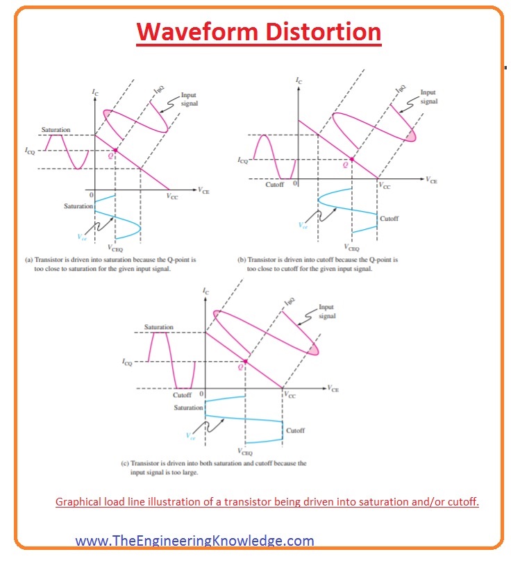
So why the distortion?

Let's consider a simplification - using solid state. Source:https://www.theengineeringknowledge.com/transistor-dc-operating-point/
Waveform-Distortion.jpg


The sound input sine wave comes in (that's the input signal above) which results in current and voltage signal. The load line that cuts across the graph through the centre point Q. This line is dictated by the resistance of the load the tube output is driving, the voltage (ie the 150V or 320V I talked about) and the current - this is where you'd set a milli-amp idle point for the tubes.

A low impedance output means that load line will appear vertical - giving a large current change but small voltage movement (although to get the current through the resistance of the headphone it needs more voltage than your headphones state).

The above is simplified because the input to load line is linear (straight and equal on the up and down of the wave). Looking at a tube example from turner audio (source: http://www.turneraudio.com.au/OTL-amps-pros-cons.html ) shows why the OTL is difficult and extremely power inefficient:
images


You can see the lines for an output power tube - the sloped 0, -10, -20V etc are the tube's input lines and they're not linear as there's differing space between them. On this you can see also the maximum power which drops down is the maximum current*voltage power the tube can deliver.
The set of colourful lines show the resistance (or reactance) governed load lines for different impedances. As headphones vary in resistance (impedance) over frequencies, this is not quite as simple as it seems.

Things like push pull, class AB1 etc all add complications to the design and fundamentally complicate the calculation of the load lines (class AB1 for example has a kink in the load line that you try to bend around the maximum power line.

Even harmonics are created by non-symmetrical output - ie the input is distorted by the tube characteristics causing the top of the wave to be higher than the bottom of the wave is lower than the centre point.

Odd harmonics are created by symmetrical output or distortion such as the same distortion above and below the centre point - in class B that's kinks causes by amplifying the top and bottom separately for example.


So designing an amp is taking each tube's load lines - input to output, output to input.. to create a amplification of the signal with minimal distortion. The couple that with removing/cancelling noise.
 
Last edited:
I've got the go-ahead from the boss.. so I'll be ordering some hardware soon :)

* 3x ecc99
* 2x 12bh7
* 5x B9A
* 6x IXCP10M90S (two per channel, and two in reserve current limit. They can cope with 300mA 40W and 900V max but 100mA sustained - more than enough. Heatsinked.
* 2x 10Kohm wire wound resistors for plate adjustment
* 2x 1Kohm wire wound resistors for CCS adjustment
* fixed resistors
* 450V coupling caps
* 450V output caps
* heater wire
* signal wire
* RCA socket
* headphone socket
* 230 to 200V trafo for B+
* Bridge diode
* Smoothing caps
* LM315 regulator
* power stage caps (ie between each second as the ground loop returns to the cap)
* Volume pot
* fast blow 350V 100mA fuses
* solder
* 32ohm test speaker

Trying to think of anything else.
 
Last edited:
I’ve been planning out the power, or at least researching it.

It’s relatively simple to make a 200V unregulated supply, but what I don’t want todo is simply use a resistor to drop 50V given the 150V B+ rail will be 150mA but specced for 300mA - 50*.3 is 15Watts of heat!

There’s a number of ways to boost the voltage, a 50V secondary could be added in series with a 150V secondary to get 200.. then the fun starts.
The voltage drops - first across the rectification, then across regulation. I decided that regulation would be good, given if you go with unregulated you have to compute the voltage drop when the load is attached (ie the amp).

I’ve modelled a transformer LTSpice, so I will build up a regulated supply and work out how to get a the two voltages without wasting too much.. however regulated means putting a heatsink somewhere in the physical design.
I also thought that DC heaters (12.6V 2.5-3A) perhaps from a separate transformer - connected so they’re not floating, that way I can put the heater power elevated just a little (the cathode sits about 8-20V) not strictly needed but I hear it helps reduce hum/noise.

the power needs to have some wiggle room, the amp finer tuning for the valves is needed as each valve differs and the LTSpice model is good to get a general ball park. So then all the resistors are variable until a good operating point is found.

I’ve also tried drawing out point to point wiring.. and to make it easier it may be better to have equal valves - instead of 3 tubes output - ie one tube has both channels to simplify the wiring have left and right with 2 output tube each - then simply wire the unused triode to ground. With 4 triodes it would have to idle at 100mA per channel so not connecting the 4th reduces current to 75mA idle.
It also means the two channels are kept separate. Like monoblocks, making the wiring separate for each channel.

Then, I will add in a soft start with mute etc as the modelling has shown a 90V spike at power up. Valves start and if the grid is 0V and the B+ rises then the valve is wide open allowing maximum current - even beyond the power handling of the tube. Having a soft start compounds that risk as the start takes longer, so the idea is to soft start until the caps etc and regulation is ready then simply switch on the heater, grid bias and B+.
The design has a cathode sit at 8-20V so it’a possible to let the cathode rise quickly setting the bias instantly but the risk is a current spike - something I need to model a bit more. Old valve regulators took their time to start, hence a ramp up, so I need more thinking in this area too.
 
Back
Top Bottom