You are using an out of date browser. It may not display this or other websites correctly.
You should upgrade or use an alternative browser.
You should upgrade or use an alternative browser.
PARVUM LIGHTNING
- Thread starter JR23
- Start date
More options
Thread starter's postsAssociate
- Joined
- 24 Apr 2012
- Posts
- 810
- Location
- Carlow, Ireland
Stunning work man!
Associate
- Joined
- 10 Nov 2009
- Posts
- 118
- Location
- Doncaster
Absolutely stunning piece of craftsmanship.
For me it wouldnt be about the cost of this build, it would be the fact i could turn around and say, i've designed this from scratch, took CAD and turned it into reality. I hope your sponsors are as happy with this as you are.
JR23, looking forward to see what you do next..
Associate
- Joined
- 14 Aug 2014
- Posts
- 1,070
Everything on the inside of that case looks positioned perfect to the millimetre. Great work OP. So clean.

Just one more little detail to address was the very stock Filco USB cable so I ordered a dank one sleeved in black Teleios from Pexon PC's. With lots of options to choose from I figured this would best match the build and the keyboard.
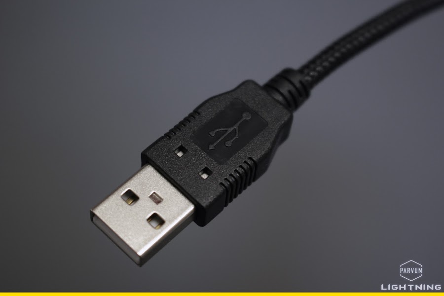


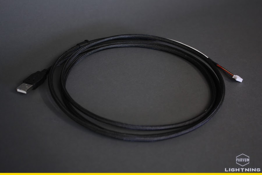
Fitting it was a bit too awkward to photograph as my Filco didn't want to split completely in half, rather than scratching the front edge trying to get it to unclip I just gently slid the cable in from the back edge.
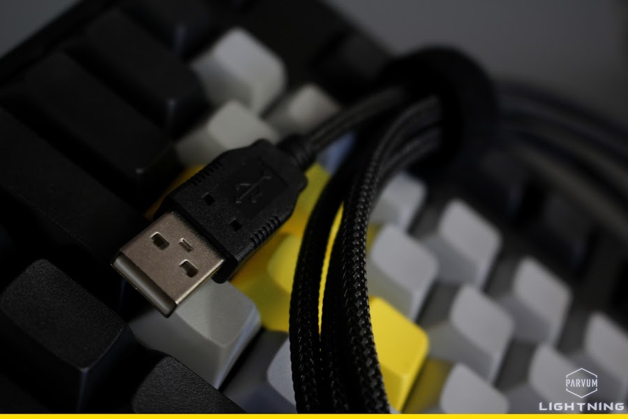
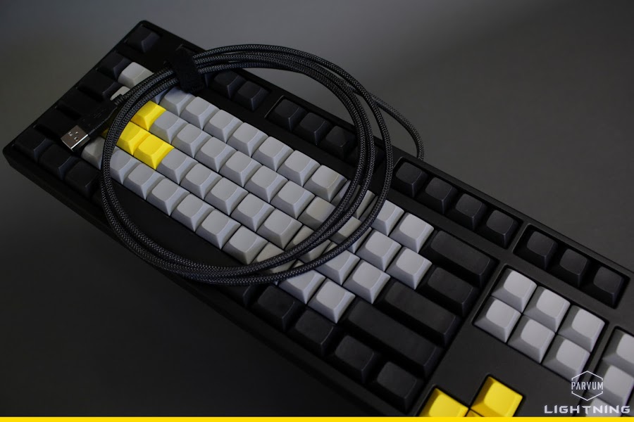

Top work from team Pexon! I'm really enjoying using this keyboard and i'm glad that I went for MX-blues the light tactility is well suited to my mashing style. I've started to use Lightning a little with a 32" 4k IPS AOC and GTA V is looking absolutely epic although something isn't getting on with Windows 10 and causing occasional freezes in game. It's got a few shows to attend over the coming weeks, one quite close to our friends studio so final photographs have been put on hold until then, i'll make sure to get lots of teasers at LSUCS LAN and PC Gamer Weekender though!
JR
Stunning work man!
Thanks!
Just keeps getting better... Great work!
Keeps getting yellower and blackerer.
Absolutely stunning piece of craftsmanship.
For me it wouldnt be about the cost of this build, it would be the fact i could turn around and say, i've designed this from scratch, took CAD and turned it into reality. I hope your sponsors are as happy with this as you are.
JR23, looking forward to see what you do next..
I know MSI and Noctua love it, HyperX just replied with 'want!' last time we updated them, but I hope they are pleased too. It looked phenomenal at i56, I'm sure all the OCUK crew would have taken it home. The next project for me PARVUM FURIA is in motion, expect something very different.
Everything on the inside of that case looks positioned perfect to the millimetre. Great work OP. So clean.
Yeah, it wouldnt of fitted if not
 the layout was devised over a year ago just as a hypothetical day dream, I never thought that I would have the chance to make it without compromise.
Look forward to seeing the final shots.
So close, more teasers and event photos first though!
JR

A couple of shots of LIGHTNING in action.


I swagged a 32" 4k IPS AOC and have been putting some epicly pretty GTA V hours in. After a huge beef between nvidia drivers and Windows 10 things are finally running right and its glorious.
JR

LIGHTNING, αclass and I just got back home from an awesome weekend at LSUCS Charity LAN 56. Much chocolate was consumed, chats were had and rather un-ordinarily multiplayer games were played with other people actually present!

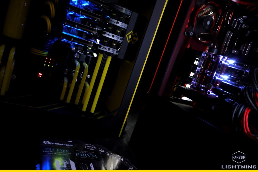
After an initial and expected battle with Windows 10, which still thinks it knows best about drivers, both rigs ran very well. AOC kindly sent Parvum a few samples from their awesome IPS range so I picked out my favorite the 32" 4k to take along and stress LIGHTNING with but quite frankly the shear number of pixels was no match for 4 GK110-4250-B1's. GTA V looked epic as always and I also played some Vanishing of Ethan Carter for the UE4 greatness as well as my all time favorite LAN title Unigine Valley.
agar.io also very good at 4k!

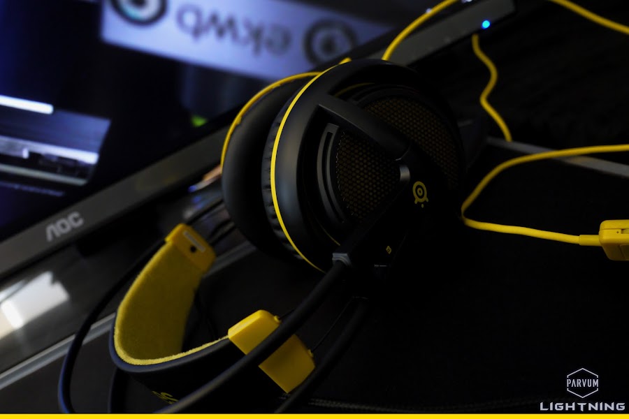
Also I got a little more accustomed to my new Filco making a few forum posts and totally not having a Fast and Furious related meme war. As well as the Filco I tried out my gift from OCUK, the steelseries black and yellow thingy's. While less comfortable and pleasurable than my Beyers they are much better suited to the LAN environment than a condenser mic and open backs.


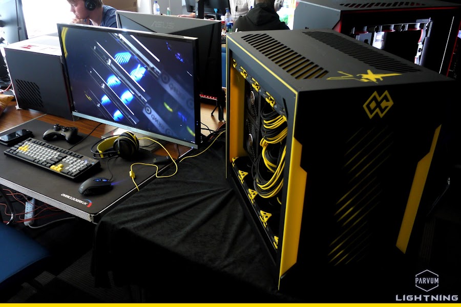

On the way home I managed to fit both rigs in my car although with no room left for monitors I may need to re-think my LAN setup for longer distances and maybe not take two giant ATX rigs. It was great fun and I can't wait for the next event!
JR
Last edited:

A long long overdue update on LIGHTNING! Even though the system has been up and running for several months now I was overcome by a sudden urgency to extract just a little more performance. Who knows why, perhaps computex, maybe pascal or it could just be the need play with some Quad-SLI insanity with all this foolish chat of its demise.

www.3dmark.com/fs/8687219
After several attempts with different overclocking utilities, different drivers and piddling with a few other factors I eventually succeeded in breaking the 30k barrier with a clock speed of 1215/1750 on all 4 cards. Definitely an impressive score however I knew at least a couple of the cards were capable of more. So off I went to find the limits of each card under water...

ASIC Quality (%) - Max Core Frequency at stock volts (MHz) - Heaven score (fps)
So after a little testing I found that one card was much weaker than the others, one incredibly fast but inefficient and two somewhere in the middle. Although I had tested each card on air originally I really didn't pay attention to where they were placed on the board. Consequently with this new found knowledge it was decided that there probably was a more efficient order to go with.

Naturally this meant it was time to tear down the GPU loop and mess around with the placement of each card. Not a small task but actually quite a fun one and a decent opportunity to take some photographs of LIGHTNING in pieces.

Because it was originally assembled very quickly in time for insomnia I never had chance to show much of how it fits together so this should be quite insightful and a great chance to give everything a good clean ready for the next season of excursions and shows.


With the rearmost black panel removed all of the screws which secure the PSU's and GPU's are exposed. Once removed the yellow and grey rear panels can be taken off making it easy to swap around the cards.

And relatively quickly the back end of the case is removed


Time to take some cards out and already barely visible bits of hardware start to surface!

A motherboard, complete with chipset heatsink and M.2 drive! I knew it was under there all along.
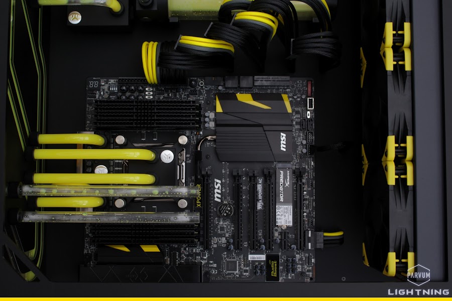
With the back off and the cards out many other new sights appeared.

But it was time to start putting them back.


Lovely EK-HD fittings made it all so easy.
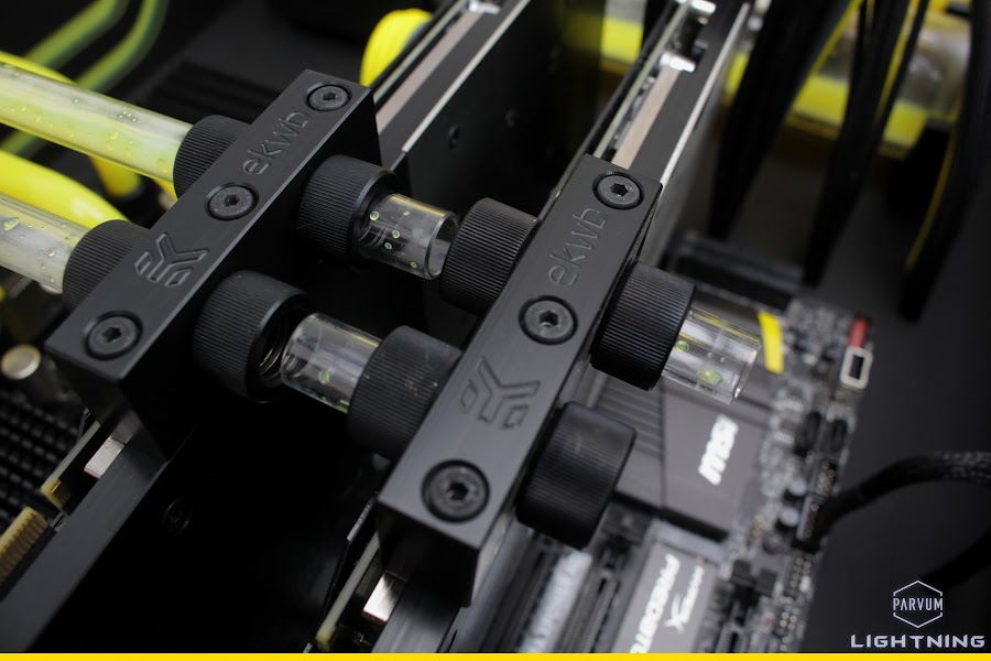
Bye bye M.2! Maybe I will see you again next year.

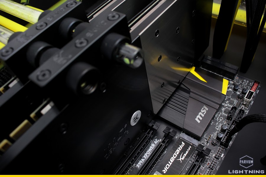
While putting back the final card I did a little oops and spilled coolant on the rear bank of memory. Nothing a few minutes with the hair dryer and a clean couldn't recover.

All neatly back and ship shape tucked right up to GPU1.


GPU1 check... GPU2 check... GPU3 check... GPU4 check... oh great, they all made it back.

Last chance for some weird perspectives before the case is reassembled.


Finally time for coolant again, the original pastel yellow still looks perfect, identical to the CPU loop, so back in it goes!

POWER!


Time for more tweaking!

Now the weak card is in the slot closest to the CPU followed by the two average ones and finally the fastest card furthest away.

www.3dmark.com/fs/8784147
The best score I got out of it at stock volts with the new GPU order was 31'782, a considerable gain. Now time to ascend to the realms of some serious overvoltage I think!
JR
Soldato
- Joined
- 1 Dec 2015
- Posts
- 18,512
I have a feeling this post may cause a lot of system rebuilds over the weekend 


