• Competitor rules

    Please remember that any mention of competitors, hinting at competitors or offering to provide details of competitors will result in an account suspension. The full rules can be found under the 'Terms and Rules' link in the bottom right corner of your screen. Just don't mention competitors in any way, shape or form and you'll be OK.

** The Official Nvidia GeForce 'Pascal' Thread - for general gossip and discussions **

bru

bru

Soldato
Joined
21 Oct 2002
Posts
7,359
Location
kent
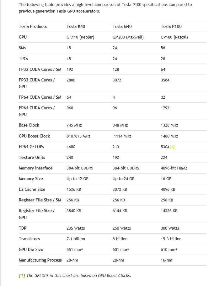
Here is the latest info on Pascal P100.

Tesla-P100.jpg


Taken from here.

https://devblogs.nvidia.com/parallelforall/inside-pascal/
 

bru

bru

Soldato
Joined
21 Oct 2002
Posts
7,359
Location
kent
Looks like a monster for gaming though, shame it's so far off.

Bear in mind this is not a consumer part this is a Tesla specced part, not even a Quadro part.

Of course having said that the underlying structure of the chip will be the same, but I would expect clock speeds to be very different. for example the GK110 Tesla part was clocked at 745MHz whereas the 780ti came in at 876MHz, the GM200 Tesla part 948MHz whereas the 980ti 1000MHz and we all know that custom AIB raise the base clocks as far as they can, near 1200MHz base clocks for 980ti's are not uncommon.
Maybe this will mean will see a 2 GHz card when these finally make it to market in consumer form.
 
Caporegime
Joined
18 Oct 2002
Posts
33,188
Looks like a monster for gaming though, shame it's so far off.

It doesn't, it's huge and has 3 times the DP performance of GK110, but only just over twice the SP performance. 580 > Titan had basically 3 times the SP performance. It looks a heavily compute performance increased card and one of the smallest jumps in SP(mostly gaming) performance in recent history.

Bear in mind this is not a consumer part this is a Tesla specced part, not even a Quadro part.

Of course having said that the underlying structure of the chip will be the same, but I would expect clock speeds to be very different. for example the GK110 Tesla part was clocked at 745MHz whereas the 780ti came in at 876MHz, the GM200 Tesla part 948MHz whereas the 980ti 1000MHz and we all know that custom AIB raise the base clocks as far as they can, near 1200MHz base clocks for 980ti's are not uncommon.
Maybe this will mean will see a 2 GHz card when these finally make it to market in consumer form.

K20 was 225W while Titan was 250W and came significantly later. This time Nvidia are rating their professional card at 300W.... meaning there is pretty much no reason to expect these to have a higher clock speed at all and no, no way will you see a 2Ghz part. This card is already running hot at the current clocks and there is little to no reason to expect higher clocks. In fact they could well go down to 250W for a consumer card.
 

bru

bru

Soldato
Joined
21 Oct 2002
Posts
7,359
Location
kent
K20 was 225W while Titan was 250W and came significantly later. This time Nvidia are rating their professional card at 300W.... meaning there is pretty much no reason to expect these to have a higher clock speed at all and no, no way will you see a 2Ghz part. This card is already running hot at the current clocks and there is little to no reason to expect higher clocks. In fact they could well go down to 250W for a consumer card.

Good point I didn't notice that. At 300W this seems a bit disappointing, I'd even go as far to think that something doesn't seem to add up.
 
Associate
Joined
8 Jan 2014
Posts
445
I would think Nvidia would come up with something more imaginative than 1070 :)

No point in 0. Call it 170 and it makes more sense.
 
Last edited:
Man of Honour
Joined
21 May 2012
Posts
31,922
Location
Dalek flagship
Good point I didn't notice that. At 300W this seems a bit disappointing, I'd even go as far to think that something d;oesn't seem to add up.

Whack a waterblock on it, job done.

Try overclocking a 5960X, 300W is nothing compared to that.:D

Almost forgot, the midrange cards we will see this year will be half the size and use about 150W so it is not all bad news.
 
Soldato
Joined
7 Feb 2015
Posts
2,864
Location
South West
Very surprised that they jumped to 600MM^2 so fast. But it appears that they needed to since they have used dedicated DP units again.

I can see vega being around 300 - 350mm^2 with more SP and DP performance than GP100 if it has 4096 SM's like the leaks mention. The size of the core would not be too much bigger when adding DP support back considering the way AMD perform DP compared to Nvidiaa.

I can also see GP100 not coming to desktop but instead them giving something between GP104 and GpP100. Like GP102 or something which has no DP units in hardware and has SP SM's instead. A part made for SP performance that would surpass GP100 in SP performance.

GP100 would not be a very good gaming part on the desktop for what it is. At the size of die it is and with just under 1/3 of its area dedicated to DP hardware. it would not be as good for gaming as the Titan X was.

IF it does come to desktop it will be a very expensive Titan card, more so than the current and past titans. Unless they have some very good yields already on FF+.
 
Associate
Joined
26 Mar 2016
Posts
150
I also don't believe in Desktop GP100. This gpu has only one real goal and this is to fight Xeon Phi. HPC stuff is taking way too much space in this gpu for consumers.
 
Caporegime
Joined
18 Oct 2002
Posts
33,188
Good point I didn't notice that. At 300W this seems a bit disappointing, I'd even go as far to think that something doesn't seem to add up.

Honestly could be as simple as needing that much to give it a none awful FP32 performance increase. IE if this was a 225W card with 1Ghz clocks, TF performance would be what under 10TF, not that far ahead of a last gen Fury X... it's still notgreat but I can understand that making a higher power card to extend the gaming/FP32 performance gap between their generations is fairly important to not be seen as stupid cards.

There is also the fact it's a HBM2 card. Simpler layout, smaller PCB, for a similar sized card they can afford to stick a lot more heatsink within the same area. They might simply be more comfortable cooling this card at 300W than a normal card at 225W.

Maybe it's a bit of both, a lot of the numbers are weird from what we're getting. Drive PX2 numbers are just freaking weird, making absolutely no sense at all. GP100, you would certainly expect (based on existing trends) for a smaller TDP card and lower clocks for more efficient power.

Could be down to the process and where it's most efficient. Say that at 1v the card can't break 1Ghz and uses 250W, but with only 1.1v it can work fine up to 1350Mhz and only uses 300W to do so, so 20% more power for 35% more performance. It could just be that those clocks and 300W is where it's best performance/watt happens to be at.

Could be all of them, or none of them.
 
Caporegime
Joined
18 Oct 2002
Posts
33,188
Anandtech have an article up... another very odd number now. The memory is clocked at 1.4Gbps rather than 2Gbps. HBM1 being 1Gbps. When I saw the 720GB/s bandwidth with 4 stacks I initially figured ECC memory might account for a large memory bandwidth reduction though it seemed excessive or that Nvidia were randomly listing effective bandwidth(all gpus/cpus have significantly lower effective than max theoretical bandwidth).

But with HBM2's main thing being 2Ghz instead of 1Ghz clocks... 1.4ghz is odd. More fine grained memory allowing them to simply pick and choose the exact amount of memory bandwidth they need and push more power to the cores? Samsung HBM2 having issues hitting 2Ghz clock speeds, 8 hi stacks proving more difficult than they hoped with temps at 2Ghz or maybe memory controller unstable at 2Ghz on Pascal.

I'm surprised they wouldn't just advertise 1TB/s and have the memory downclock for efficiency reasons because, frankly 1TB/s looks really impressive and iirc Nvidia have been calling Pascal a up to 1TB/s architecture for the past couple of years. It does feel more like a forced decision rather than active choice.
 
Back
Top Bottom