• Competitor rules

    Please remember that any mention of competitors, hinting at competitors or offering to provide details of competitors will result in an account suspension. The full rules can be found under the 'Terms and Rules' link in the bottom right corner of your screen. Just don't mention competitors in any way, shape or form and you'll be OK.

** The Official Nvidia GeForce 'Pascal' Thread - for general gossip and discussions **

Soldato
Joined
7 Feb 2015
Posts
2,864
Location
South West
That seems to make sense, I assume that the mixed precision stuff they talked about wouldn't allow then to use the 1*64bit units to output 1*32bit results and that it is related to something else?

Nah, the DP unit seems to be pure 64bit work. Only the SP units seem capable of performing two 16bit int instructions perclock. I believe the mixed precision comes from the ability of the GPU to run 16, 32 and 64 bit instructions simultaneously. Although it could just be talking about the SP units being capable of 16bit int instrucitons.
 
Associate
Joined
13 Oct 2011
Posts
1,419
Location
Suffolk
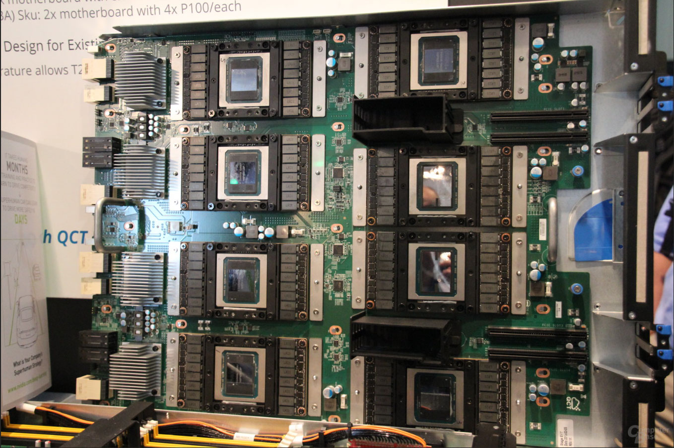
Great find there and a couple of pics for those who might not have clicked on that link.

DGX-1.jpg

Goes to show that they have actual chips in house and the DGX-1 systems built up for testing at the very least.

Anyone else notice that there seem to be 2 different chips in that photo? The two in the middle on the right seem to have a shiny look across the whole chip, the others the memory chips look small/dull.

If you read the link they suggest the dull ones are HBM1 based ones as nvidia only recently got HBM2 samples. If they only have a couple of HBM2 GP100 examples it feels like they have been a bit deceptive about how ready it is.
 
Soldato
Joined
7 Feb 2015
Posts
2,864
Location
South West
Those ones in shot are labeled weeks 41 and 45 from last year. They are more than likely very early engineering samples that might not even work. And since they are displaying old hbm 1 based samples and there seem to be more in that box than hbm2, they might not have many gp100 ready.

Or they just decided to stick duff ones in that just as a mockup I anything. Apparently they only had one working dgx1 unit on show at the event. So backs up that they don't have many fully working units yet.
 
Caporegime
Joined
18 Oct 2002
Posts
33,188
Anyone else notice that there seem to be 2 different chips in that photo? The two in the middle on the right seem to have a shiny look across the whole chip, the others the memory chips look small/dull.

If you read the link they suggest the dull ones are HBM1 based ones as nvidia only recently got HBM2 samples. If they only have a couple of HBM2 GP100 examples it feels like they have been a bit deceptive about how ready it is.

considering HBM1 and HBM2 have different heights as well, it seems fairly unlikely the packages would look the same bar different size of memory chips.

Not saying they are fake, though it wouldn't remotely surprise me if they were non working and the number of real working samples is insane. Personally with them announcing an intention for actual availability in Q1 and just potential availability before that, that they are expecting 480 gtx levels of working chips back in the mean time. Pick a high end partner who wants them, get them to sign a NDA whereby they ship them 5 a month from June for free with a bunch of free GK110 cards upfront and 1000 free next year and they publicly claim their needs are being met from June. Nvidia then get to claim they are shipping from June even though any other company would count it as shipping samples to a partner and count the launch as Q1 next year.


Will be very interesting to see if the final chips look the same or if the chips look closer to Fiji interposer designs within the infilling around the chips.

As others have said, it could be more than possible that they don't ship this as a consumer/gaming part. If they do, while faster, it doesn't look like it would be a beast for gaming. If they make entirely different parts for gaming it will then become interesting to see what they do, will a gaming part be similar but compute stripped out and 30% smaller, or will they make an entirely different 600mm^2 chip for gaming.
 
Soldato
Joined
7 Feb 2015
Posts
2,864
Location
South West
Will be very interesting to see if the final chips look the same or if the chips look closer to Fiji interposer designs within the infilling around the chips.

As others have said, it could be more than possible that they don't ship this as a consumer/gaming part. If they do, while faster, it doesn't look like it would be a beast for gaming. If they make entirely different parts for gaming it will then become interesting to see what they do, will a gaming part be similar but compute stripped out and 30% smaller, or will they make an entirely different 600mm^2 chip for gaming.

I think that with nvidias current architecture, the best thing for them is to fully differentiate products. GCN is far more scalable in comparison without its need for dedicated DP units. Although it still needs some extra circuitry to support the DP operations. Just nowhere near as much as what a whole dedicated DP shader needs. I would say that in compassion, the amd method is probably just larger than two SP shaders. But was still enough to push the size limit for fiji when that extra size from the supporting DP enabling hardware was added up.

Also on the interposer note, i think it is just that they have made the interposer as large as possible to just fit a 600m^2 chip and the four HBM2 4hi modules. So they have made it as flush as possible since it is already a very large and expensive interposer and die.

Although i though fiji supported 1/2 DP in hardware they must have cut out a lot of the support circuitry in the end to keep it under 600mm^2. it would more than likely have been knocking on 650mm^2 with it all, beyond the size limit.

I reckon Vega will be quite a monster part, all while being near half the size of GP100. Yet it will more than likely exceed it in terms of SP and DP performance. maybe even by double depending on clocks and how much extra performance GCN4.0 brings. Considering fiji already has 8Tflops SP at 1ghz. clock that up to 1.4-1.5 like gp100 and you already have 12Tflops SP, more than GP100 and that is before any improvements with GCN4.0 SM's.
 
Last edited:
Associate
Joined
24 Jan 2016
Posts
527
Location
Sheffield
I for one wouldn't mind if the next titan had the GP100 base to be honest.
Could do with the extra 64bit units.
I don't use my cards for just gaming.
 

Mei

Mei

Soldato
Joined
3 Jan 2012
Posts
3,980
if uni's have to wait atleast 6months for it i dont see gamers getting it any sooner
i think we in for a bit of a wait :(
bored of this gen of cards i want the new stuff :(
 
Soldato
Joined
17 Jun 2004
Posts
7,617
Location
Eastbourne , East Sussex.
The Tesla P100 package includes four 4-Hi HBM2 stacks, for a total of 16 GB of memory, and 720 GB/s peak bandwidth. That’s three times as much bandwidth as Nvidia’s previous flagship accelerator the Tesla M40. The Telsa P100’s bandwidth figure is below that of the JEDEC HBM2 spec that SK Hynix & Samsung both adhere to. Which dictates that every 4-HI HBM2 stack should operate at a 2Ghz clock speed to deliver 256GB/s of bandwidth for a total of 1TB/s for four stacks. The HBM2 modules on the Tesla P100 actually operate well below the spec at only 1.4Ghz.
This is part of Nvidia to reduce the overall power of the package, which even reduced is 300w+
 
Soldato
Joined
1 Nov 2002
Posts
10,255
Location
Sussex
Don't really understand the need to lower the TDP. What woukd be wrong with 350 (guessing) but full fat memory speed...they obviously know what they are doing. Just seems odd.
 
Man of Honour
Joined
13 Oct 2006
Posts
92,158
The Tesla P100 package includes four 4-Hi HBM2 stacks, for a total of 16 GB of memory, and 720 GB/s peak bandwidth. That’s three times as much bandwidth as Nvidia’s previous flagship accelerator the Tesla M40. The Telsa P100’s bandwidth figure is below that of the JEDEC HBM2 spec that SK Hynix & Samsung both adhere to. Which dictates that every 4-HI HBM2 stack should operate at a 2Ghz clock speed to deliver 256GB/s of bandwidth for a total of 1TB/s for four stacks. The HBM2 modules on the Tesla P100 actually operate well below the spec at only 1.4Ghz.
This is part of Nvidia to reduce the overall power of the package, which even reduced is 300w+

Its not something I know much about and others have suggested that the difference would be the quality of the process rather than the size of the core but another company making a product on TSMC 16nm was claiming that many of the advantages over 28nm were going out the window the larger you made the chip with it tailing off steeply above 3xxmm2.
 
Soldato
Joined
17 Jun 2004
Posts
7,617
Location
Eastbourne , East Sussex.
when looking at the spec it did get me wondering what Nv are doing - as the FuryX has 512GB/s bandwidth so the 720 didn't make much sense , until I realised they were coming in a lot slower for power.

power use on large die size has allways been an issue with leakage , which would be worse when a young process gets smaller
 
Man of Honour
Joined
13 Oct 2006
Posts
92,158

Mei

Mei

Soldato
Joined
3 Jan 2012
Posts
3,980
Kind of annoying my 780 is a fairly decent clocking card and handles everything fine aslong as I avoid 4K which makes it hard to justify spending money on anything else out now.

annoying for me too, my roomie has a 980ti :mad:
its probably worth waiting now if just for the new connects on cards!? especially on the AMD cards
and nvidia might have new displayport!? i duno
 

bru

bru

Soldato
Joined
21 Oct 2002
Posts
7,359
Location
kent
Those ones in shot are labeled weeks 41 and 45 from last year. They are more than likely very early engineering samples that might not even work. And since they are displaying old hbm 1 based samples and there seem to be more in that box than hbm2, they might not have many gp100 ready.

Or they just decided to stick duff ones in that just as a mockup I anything. Apparently they only had one working dgx1 unit on show at the event. So backs up that they don't have many fully working units yet.


That's good, at least they do actually have them up and running then.
As for that backing up they don't have many working units, well it might do but then how many do you need to show people before they believe you have them up and running.
Does that mean that AMD only had very few Polaris 11, when they did the Capsican event seeing as they only had one running, of course it doesn't. It just means that here is one running to show you that it actually works.

And before we go down the route of it might have just been a box with other parts inside, I said the same thing about the AMD event and was told it is not possible to fake it. But yes it might have been faked, but I do sincerely doubt it.
 
Associate
Joined
25 Dec 2008
Posts
187
just a thought - the PC games market is not that huge (compared to other markets) these days.

I reckon new architecture is heavily linked to games consoles and other industry applications. Thats why deep learning was a big thing this year - theres a need for it.

If you think about it, 4k gaming wont be mainstream until loads of people have 4k TV's and a 4k games consoles (not upscaling). Also VR is in its infancy.

These things are probably a few years off from maturing, so if you were a graphics chip company - gaming is probably not your biggest priority this cycle.

Why put the investment in for 2016 for new graphics chips when the market isn't ripe - just keep researching, tweaking etc - then release a big leap in 2017/18.

just a thought that crept into my mind.
 
Caporegime
Joined
18 Oct 2002
Posts
33,188
For their last quarter of 1.4billion income 810mil was graphics, the other segments all together weren't close to as big and the biggest non gaming segment was worth 203million income. Gaming is by a huge margin their biggest earner.
 
Back
Top Bottom