• Competitor rules

    Please remember that any mention of competitors, hinting at competitors or offering to provide details of competitors will result in an account suspension. The full rules can be found under the 'Terms and Rules' link in the bottom right corner of your screen. Just don't mention competitors in any way, shape or form and you'll be OK.

AMD Navi 23 ‘NVIDIA Killer’ GPU Rumored to Support Hardware Ray Tracing, Coming Next Year

Status
Not open for further replies.
What are you talking about?
I'm talking about die size.

Nvidia lost their Efficiency per mm2 a long time ago? That they need to pack on more transistors to maintain a competitive edge? Lets look at those claims by comparing some of the like for like GPUs.
I consider 2-3 years long time ago.

28nm Fiji and 980ti.

Fiji: - 596mm2 and 8.9 Billion Transistors
980 T:.- 601mm2 and 8 Billion Transistors.

So Nvidia has the edge here. And not only has the edge in efficiency per mm2 but also has better performance and consumes a lot less power.

14/16nm: Pascal and Vega.

Vega 64: - 486mm2 and 12.5 billion Transistors.
1080: - 314mm2 and 7 billion transistors

So, Nvidia is way more efficient per mm2. Performance is about the same with Vega getting a little better towards the end. I am also going to say power consumption is roughly the same too as you can under volt the Vega cards.

The current situation is that Nvidia are still on a 12nm process and AMD are on a 7nm process. Also, AMD's current GPUs lack any support for any of the Directx 12 Ultimate features. So you won't be able to make any meaningful comparisons about efficiency until both companies are on the same die size and pushing the same features (DX12 ultimate)
That's some good fishing expedition. Since it's apparent that you won't be buying those cards this or next generation going back then serves little relevance to Navi, Turing and Ampere (that I was making reference to). Lets try to keep the conversation current.

I think most people on this forum don't mind the power consumption as long as the performance is there. And that's where AMD have been failing. Their GPUs use a lot more power for less performance than their Nvidia counterparts. Or to put it another way, if AMD came out with a 250Watt GPU that smashed the 3080TI, nobody here would care that it used 300Watts.
This is a myopic statement there. GPUs require power regardless be it more or less. And like you said most don't mind the power consumption as long as the performance is there. It's doesn't necessitate how "you" define that performance. Why? Because you left out one very important aspect, price. Therefore, it's not power consumption that takes focal point, it's the price. Making that statement moot.


This whole section of your post is inaccurate. Oh, what you are saying is correct about more dies per wafer been cheaper etc. But, the basis for this is all wrong. You are looking at Navi cards on a 7nm process and comparing them to Turing on a 12nm process. Do you really think that AMD's big Navi will be competitive with the 3080Ti and still be the same small die size as the 5700XT? Not a hope.
You can't say it's accurate then say its inaccurate for the sake of saying "it's inaccurate". It's not about the differences in Uarch on the wafer as you speciously claim. It's about the manufacturing cost per wafer that I was referring to. We know that nvidia is going to 7nm. It's pretty much a given that the die sizes on Ampere will mimic Turing (and yes that is my opinion on it). Lets stay on topic here.

We can even work it out. The Xbox series X has an RDNA 2 GPU that's supposedly about the same performance as the 2080 super(545mm2). The GPU in the Xbox is 360mm2. But again, that's 12nm vs 7nm. So if the 3080Ti is 30% faster than the 2080Ti, then big Navi would need to be over 500mm2 to compete. And that's just in rasterized performance. They will also need to be competitive in Ray Traced performance.
Performance isn't my discussion. I clearly stated that manufacturing cost is where AMD seems to be targeting Nvidia. As you pointed out AMD found a way to bring 360 mm² die to perform about the same as 2080 which is 545 mm², on console. That's the point! AMD is focusing on area (real estate). Nvidia, performance. Yet AMD is catching Nvidia on performance while still accounting for area (real estate).

And with all this extra size and features will come extra expense. Considering the 5700T had a small die and has no support for yet cost $399 on release. And, as you say large dies cost more, so it could easily have an $800 plus price tag.
Not extra expense, area expense. The cost of those gpus per wafer along with functional gpus per wafer, etc. will provide a total cost to manufacture. Which, as we know, is trickled down to the consumer. What you pay for is not so much a luxury tax but the actual cost to manufacture. Which will always be higher. So no, Nvidia won't be able to cut prices if AMD does have an answer to Ampere Titan (IMO). Which is the rumor. That's why I made the correlation between AMD vs Intel and AMD vs Nvidia in my earlier post.

As for Dx12 Ultimate, sure it's unfortunate that Navi10 users don't have this. However, it's something that won't be seen in games for sometime now. Lets not confuse announcement of Dx12 Ultimate vs a game released today using Dx12 Ultimate. ;)
 
Last edited:
I'm not a fan of this unless the image quality can be proven to 100% of the time be 1:1 and/or objectively superior not just subjectively better.

My thoughts exactly. I think the DLSS feature is a great idea for gamers with lesser hardware or those chasing higher framerate, but I just feel it in my bones that it will be used in a nefarious or dishonest way to make something appear better than it is. As I've said previously, I would love to be proven wrong. Time will tell and it's not like the competition wouldn't try something similar if they had a lead to defend.
 
We can even work it out. The Xbox series X has an RDNA 2 GPU that's supposedly about the same performance as the 2080 super(545mm2). The GPU in the Xbox is 360mm2. But again, that's 12nm vs 7nm. So if the 3080Ti is 30% faster than the 2080Ti, then big Navi would need to be over 500mm2 to compete. And that's just in rasterized performance. They will also need to be competitive in Ray Traced performance.

Just thought I would point out the xbox series x is an Apu so the 360mm2 also contains the cpu. So the gpu part is smaller than 360 mm2.
 
Comparing transistor counts between companies is not totally accurate as they define transistor count differently. Some define it as active transistors,others define it as including non-active transistors. Comparing Vega 10 and the GP104 on a transistor basis isn't really doing the same thing. Vega 10 is a repurposed workstation GPU with significantly higher FP64 performance(around 3 times the performance as its 1:16 rate instead of 1:32 rate),and was AMD's first foray into a machine learning GPU. It is partially why it used expensive HBM2. The first Vega10 based GPUs launched were Radeon Instinct models which are commercial graphics cards,not Vega 64 gaming cards. They didn't have a GP104 competitor,so released it instead as a gaming product,by pushing clockspeeds. This is why it consumed so much power - it was never designed to be clocked as high as it could,and it was doing so on a worse GF process.

You only have to look at Navi10 - it actually has just over 10 billion transistors,and Vega10 has 12.5 billion transistors,but lower FP64 performance. Navi 10 beats Vega 10 in gaming performance despite having 20% less transistors. Even compared to Polaris 20,Vega 10 had 2.2X the number of transistors,but at best only had 60% extra gaming performance at 4K.

Also look at the Nvidia GM200 and GP104. The GP104 had 10% less transistors than the GM200,but beats it in gaming performance,and even FP64 performance.

It also shows transistor count isn't also going to help when comparing GPUs even within the same company!

Just thought I would point out the xbox series x is an Apu so the 360mm2 also contains the cpu. So the gpu part is smaller than 360 mm2.

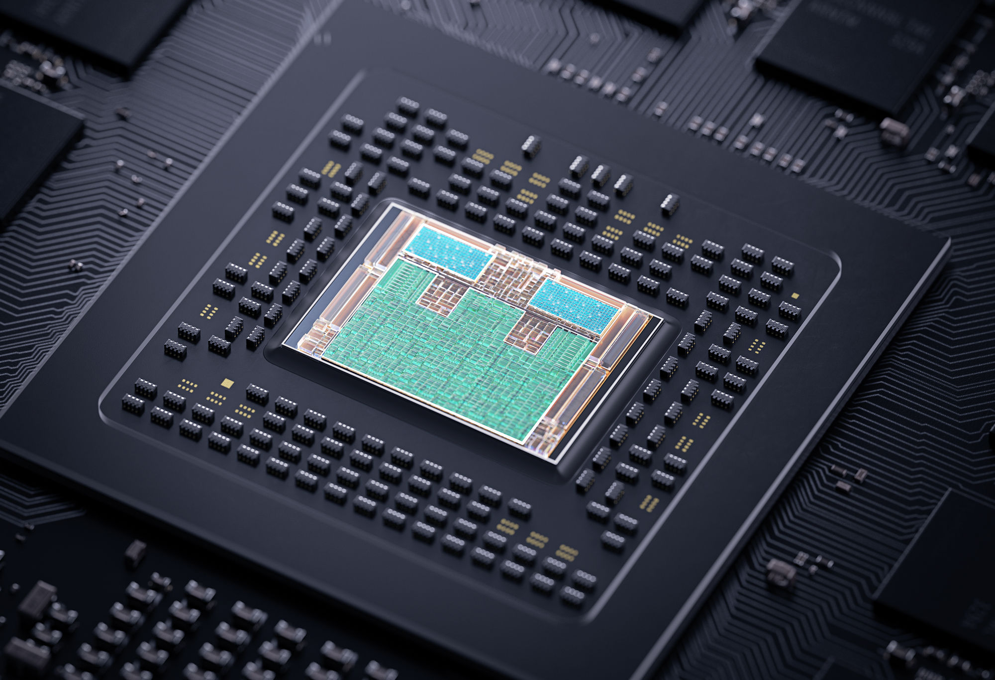
It contains the CPU,SRAM,memory controllers,audio logic,IO,NVME controler and all the other stuff.

For example,8 Zen2 cores on a chiplet are around 70~80MM2,and if the console SOCs are using the reduced L3 cache Renoir arrangement that is still at least 50~60MM2 there.

The GPU is probably well under 300MM2. There is noise that there is a Navi 22 which is around the same die size as Navi10 but also adds RT,etc.
XBOX-Series-X-SOCjpg.jpg

Looking at the highlighted parts - that looks like 56CUs,in under 300MM2.
 
Last edited:
Just thought I would point out the xbox series x is an Apu so the 360mm2 also contains the cpu. So the gpu part is smaller than 360 mm2.

Indeed. The GPU will still be 300mm2 when you factor in the extra density allowed by the 7nm Enhanced process and there is either very little or no L3 cache. But, I left it at 360mm2 because a console APU punches above it's weight as it isn't bogged down with massive OS overhead and the way the SOC is designed gets more performance than you would get in the same desktop parts.

The conclusion will still be the same no matter which numbers you use. If AMD are really going to compete at the high end they are going to need GPUs with a large die size. And large dies are expensive.

For reference A 2080Ti on 7nm would be around 471mm2.

Or do believe Eastcoasthandle and you think that AMD are somehow going to compete with the 3080Ti using small cheap dies.

No I think you are right. Amd will need something pretty large to compete at the top.
 
No I think you are right. Amd will need something pretty large to compete at the top.

The bigger the die the worst the yields though. The issue,is you only have to look at the GA100 - it is severely cut down,and has increased TDP by a significant amount. That indicates to me around 800MM2 is starting to push things a lot,even with TSMC 7NM being out since 2018.

This is why a lot of enthusiasts on OcUK,don't seem to understand why Nvidia was launching smaller dies first with Kepler and Pascal. In both cases they were the first new Nvidia consumer GPUs on "new" nodes,and the larger GPUs followed over 6 months later. It wasn't just about milking but about supply,but the milking was more the tiering of the GPUs.

So even if Nvidia is going to try and go past 600MM2,they will hit the same problems,and have people not realised,that Nvidia has tended to keep it's top consumer GPUs at under 600MM2. They seem to oscillate between 470MM2~600MM2. The median seems to be around 550MM2 IIRC.

Turing was on a special version of TSMC 16NM,ie,TSMC 12MM which increased the maximum die size you could build,etc and by then 16NM was quite mature,and the process was cheap. It wouldn't surprise me with Navi being quite an early 7NM GPU,that TSMC 7NM was a bit pricey,so costs were not as low as expected. Remember,AMD is selling 70MM~80MM2 single chiplet 7NM CPUs for upto £300.

So all this talk about Nvidia just using massive dies,means diddly squat,if yields are rubbish and the GPUs cost £2000 and people have long waiting lists for stock. The important metric will be the sub 600MM2 dies,since those are where most of the consumer GPUs will be targetted at,if not for yields but also for costs. Nvidia also operates at higher margins than AMD too. So in the end its going to be down to uarch. As shown by some examples,die size is never a good measure of performance,let alone transistor count. Both AMD and Nvidia have had lower transistor count new generation GPUs, handily outperform previous generation GPUs with more transistors and more memory bandwidth.

Another area will be software support,ie,getting your features supported by game developers. That impacts performance too. It's not just hardware too. If AMD don't get proper hardware support,it will make the theoretical performance and realworld performance not match up again.
 
Last edited:
The bigger the die the worst the yields though. The issue,is you only have to look at the GA100 - it is severely cut down,and has increased TDP by a significant amount. That indicates to me around 800MM2 is starting to push things a lot,even with TSMC 7NM being out since 2018.

This is why a lot of enthusiasts on OcUK,don't seem to understand why Nvidia was launching smaller dies first with Kepler and Pascal. In both cases they were the first new Nvidia consumer GPUs on "new" nodes,and the larger GPUs followed over 6 months later. It wasn't just about milking but about supply,but the milking was more the tiering of the GPUs.

So even if Nvidia is going to try and go past 600MM2,they will hit the same problems,and have people not realised,that Nvidia has tended to keep it's top consumer GPUs at under 600MM2. They seem to oscillate between 470MM2~600MM2. The median seems to be around 550MM2 IIRC.

Turing was on a special version of TSMC 16NM,ie,TSMC 12MM which increased the maximum die size you could build,etc and by then 16NM was quite mature,and the process was cheap. It wouldn't surprise me with Navi being quite an early 7NM GPU,that TSMC 7NM was a bit pricey,so costs were not as low as expected. Remember,AMD is selling 70MM~80MM2 single chiplet 7NM CPUs for upto £300.

So all this talk about Nvidia just using massive dies,means diddly squat,if yields are rubbish and the GPUs cost £3000. The important metric will be the sub 600MM2 dies,since those are where most of the consumer GPUs will be targetted at,if not for yields but also for costs. Nvidia also operates at higher margins than AMD too.

Another area will be software support,ie,getting your features supported by game developers. That impacts performance too. It's not just hardware too.

Yea I agree with all that you have said. Nvidia will most likely push the limits though to make sure they are still the fastest. I dont think Amd will want to go much higher than 500mm2 where as Nvidia may push 600 mm2 for gaming parts.

What I do think is AMD will be way closer to Nvidia than they have been in many years with RDNA 2. Just a shame the pound to dollar is still rubbish so prices will still be high.
 
An 80CU RDNA2 part (Nvidia killer) should be less than 600mm2 and could cause Nvidia a shed ton of problems if it indeed exists, can be mass produced and is priced well below £1k. The top end AMD part doesn't have to out perform everything Nvidia has it just needs to get close and cost significantly less such that the Nvidia part(s) make no sense e.g. an extra £500 gets you <10% gain.

It may sound silly but I think AMD can up their margins on Zen3 and offset some of that with GPUs, but can they sell that argument to the CEO and shareholders?

I suspect that the Nvidia killer will be a low to midrange card and they'll try to take Nvidia's market share from the bottom up. Small efficient die and undercut Nvidia's pricing. The 80 CU part will command as high a price as they can get away with. I may be wrong of course ;)
 
Status
Not open for further replies.
Back
Top Bottom