OMG you can't even get it right when it's written in the blooming picture, it's not a slightly taller transistor, it's a 'slightly' taller FIN.
Look it's obvious you don't know what you're talking about so I'll try explaining it to you as succinctly as i can, GloFlo and Samsung did not have their own working 14nm FinFet.
GloFlo bought IBM's global commercial semiconductor technology business that
included IBM's existing 14nm plant AND the process, along with numerous semiconductor technology IPs.
It should be noted that GlobalFoundries had no such capabilities prior to their acquisition of IBM's plant, semiconductor manufacturing group, and IP portfolio.
Samsung and GLOBALFOUNDRIES Forge Strategic Collaboration that involved sharing existing 14nm plants, processes, and numerous semiconductor technology IPs that resulted in 14LPE (14 Low-Power Early), 14LPP (14 Low-Power Plus/Performance), 14LPC (Low Power Cost [reduced]), and 14LPU (14 nm Low Power Ultimate) in that order.
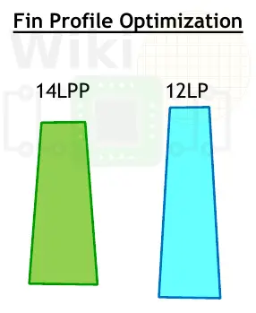
The Samsung and GloFlo collaboration on the 14LPP (14 Low-Power Plus/Performance) was used for
the original Zen, after that GloFlo building on top of Samsung's licensed 14nm process, announced the 12LP (12 nm Leading Performance) that
Zen+ was fabricated on.
Now i know that a long complicated path but saying 12LP (12 nm Leading Performance) was a tweaked 14nm, that SS 14nm vs 12nm simply has slightly smaller cells on the same substraight which gives them about 1.2X density vs the Samsung 14nm it originated from is just incorrect, it wasn't Samsung's 14nm node it was IBM's, it isn't "A" slightly tweaked Samsung node, it changed some major elements of the 2nd generation Samsung and GloFlo collaborated 14LPP (14 Low-Power Plus/Performance) node while Samsung went on to develop another two iterations of that node.
Most of what you said here is wrong AND your own links prove it.
Click your Samsung and global forge strat colab link, it straight up says this
Developed by Samsung and licensed to GF, the 14nm FinFET
Full stop, that's the end of it. Anyone not bs'ing their way through basic knowledge knows that IBMs 14nm was decent but had very different design parameters, it was designed primarily for IBM chips, that is screw power efficiency, max clock speeds were the only concern, it was more expensive and was focused on producing a relatively low number of extremely high cost server chips. It was basically unsuitable for creating more efficient higher yield cheaper chips. So straight off, and this was incredibly widely and publicly known, Global dumped IBM 14nm and licenced what was a fully Samsung process node. The original Zen was made on a purely Samsung node, developed by Samsung for mobile with the focus on efficiency and being high yielding and it went into production before Global did and it was licenced by Global. Suggesting this was originally an IBM node literally immediately highlights that you don't know what you're talking about here. Here's a hint, if one company licences a node to another company... they won't launch it before the company who actually finished it then licenced it.
Secondly, the defining characteristics on size and electrical performance come from in huge part the basic parameters of a node, the basic gate pitch, metal pitch, they pretty much define the 14nm Samsung node as what it is, 12nm makes no significant changes and ignoring the headlining numbers, 12nm is 'faster' not because it's denser, but because slightly thinner taller gates allow the chip to be less dense.
Keep in mind that Intel relaxed transistor gate pitch for subsequent 14nm nodes, that's how the clock speeds went up. 14nm had a transistor gate pitch of 70nm, 14nm + didn't officially raise it but supposedly did in the design rules, 14nm++ is a transistor gate pitch of 84nm.
Intel called all their node tweaks 14nm/+/++/+++, in the past they would have called them a new stepping on a shipping chip. With ostensibly the same cpu they wanted to make the changes sound bigger than just a stepping. With Global they wanted it to sound like a bigger improvement and they gave it a new name. It used the same equipment, it used the same patterning, it has the same physical limits, it just tweaked the design, nothing more or less. On any given set of equipment and choice of patterning you are really limited to certain physical size parameters, within those limits anyone can choose to optimise for density, voltage, performance, in fact many or most nodes do that upfront and have different designs on purpose, 14nm industry nodes were really the first where they only really bothered with one design largely because Samsung planned to go 10nm before 7nm and earlier so wasting time on extra versions of 14nm apparently didn't seem worth it to them.
https://en.wikichip.org/wiki/14_nm_lithography_process
Look at Intel, they started off, before launch, with an optimised high performance, low voltage and high density library. 12nm is nothing more than a tweaked 14nm with different design goals, using the same equipment, using the same physical limitations, using the same patterning. No one in the industry would call it a new node.
Also note the IBM 14nm, it is dramatically larger despite being 14nm, because lower density = higher performance in general. This is why Intel's nodes decreased density to raise clock speeds, IBMs node was completely unsuitable for a high volume, high yield, lower cost chip and still is, also a really really big deal here, IBMs 14nm is SOI, Samsung's is bulk, no Zen chip is produced on SOI, full stop.
https://www.globalfoundries.com/sites/default/files/product-briefs/pb-14lpp.pdf
You will notice here, particularly top of the second page, twin well CMOS bulk FinFET, with every single design parameter matching Samsung 14nm and nothing matching IBMs 14nm SOI node.


")
")