Nvidia used TSMC's foundries to fab the compute / deep learning focused GA100 Ampere chip, on their 7nm process.
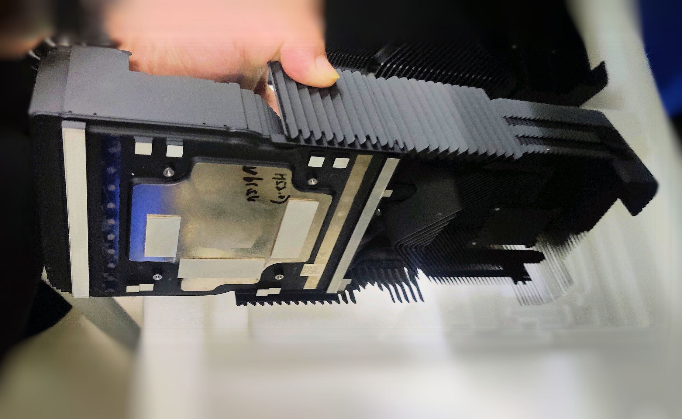
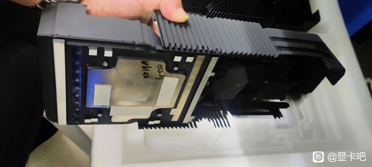
It's possible that some of the 'leaks' we are seeing are related to upcoming compute / deep learning chips.
I think they will probably use this approach again for the next series. So, compute chips will be probably be higher density + larger die size and fabbed on TSMC's 4nm process.
EDIT - Nvidia has officially confirmed that their H100 compute GPU will be fabbed on TSMC's 4nm EUV process, link here:
To power the next wave of AI data centers, NVIDIA today announced its next-generation accelerated computing platform with NVIDIA Hopper architecture, delivering an order of magnitude performance leap over its predecessor.

nvidianews.nvidia.com
Another thing to mention, is that TSMC's fabrication process costs are reportedly increasing in 2023.
Hypothetically, Samsung's 5nm EUV (5LPE or 4LPE) process should allow Nvidia to more than double the transistor density of Ampere consumer GPUs (fabbed on Samsung's 8nm).
The transistor density of the GA102 (Samsung fabbed) chip was 'just'
45.1M / mm²
The transistor density of Samsung's 5nm EUV process is upto
134.9 MTr/mm2
Info here:
10752 Cores, 336 TMUs, 112 ROPs

www.techpowerup.com

en.wikipedia.org


 That 3090Ti didn't have a long time at the top if so
  but in all seriousness i doubt we will see it come July , more likely officially announced in July with cards starting to drop in September which would be 2 years on from 3000 series but we shall see ....


