• Competitor rules

    Please remember that any mention of competitors, hinting at competitors or offering to provide details of competitors will result in an account suspension. The full rules can be found under the 'Terms and Rules' link in the bottom right corner of your screen. Just don't mention competitors in any way, shape or form and you'll be OK.

AMD Zen 2 (Ryzen 3000) - *** NO COMPETITOR HINTING ***

It can scale down but just not as well. It's about choosing your battles, i.e. where to focus engineer effort for maximum gain.

According to AMD, you can scale it down no problem, just there is no performance benefit of it so they are doing on the cheaper 14nm. If they wanted to go to 7nm they could easy.
 
It can scale down but just not as well. It's about choosing your battles, i.e. where to focus engineer effort for maximum gain.
I agree in principal, but I am not 100% sold. I have no reason to really doubt AMD but Intel have been struggling mightily with 10nm, I just wonder if there is a another reason to leaving a bunch of the process at 14/12nm.

To be fair, I dont really care overly. What is important is the single core and package performance. These chips have a really good chance of taking the lead on both fronts from Intel.

AMD still is under WSA for one,and also 7NM is probably capacity limited and more expensive per wafer when compared to 14NM/12NM. Using an older node for IO makes sense due to cost I expect.
 
AMD still is under WSA for one,and also 7NM is probably capacity limited and more expensive per wafer when compared to 14NM/12NM. Using an older node for IO makes sense due to cost I expect.

The WSA is definitely valid, I know the cost of engineering a 14nm die is less than 7nm as well. I would have expected cost to have evened out over the lifecycle - at 7nm it would be another small die, so you would expect good yields. Two fabs producing silicon for the same package has huge potential for cluck up in my uneducated opinion.

I just think that if it was feasible to have taken everything to 7nm that they would have done so. It would have been even more power efficient, they would have had all the fabrication and assembly happening at one plant.

I guess what it comes down to is that I never expect a large corporate to be completely open - or for a decision like this not to have multiple levels of complexity. It could be as simple as a reduced time to market and with the massive costs of doing anything at 7nm they may have not wanted to front foot any more development costs there than they had to plus the WSA. I just think that there might be something else at play.
 
Shrinking nodes is expensive. The benefits tend to be improved power consumption and higher transistor density, which can be used to increase performance but Intel over the last 5+ years have either struggled with this or focused efforts elsewhere (e.g. iGPU). The higher transistor density and improved power consumption might not be terribly useful for I/O. No-one seemed to question them when they claimed that it doesn't scale down as well as CPU cores and cache do, so I guess that was truthful. Essentially there are a number of reasons:

- Wafer supply agreement means they need to make 14nm dies. What else would they want to use 14nm for at this stage?
- I/O circuitry doesn't scale as well as CPU cores and cache do, and 14nm is cheaper than 7nm to produce, thus this approach saves cost for minimal drawback.
- This approach allows them to use the same 7nm chiplets for cores on Ryzen 3, Threadripper 3, and EPYC 2, which again saves cost.
- They likely expected 7nm capacity to be limited because people have been waiting for a sub-14nm node for a long time and it's new, so this approach allows them to pump out more CPUs.
- This approach also potentially allows them to produce Navi chiplets for APUs, again saving overall cost (although they've so far denied that this is their plan).
 
The power and density thing that comes from a node shrink isn't great for I/O and local memory, IIRC you get around a 10% increase in density vs the 50% for logic library's and as I/O and memory are already low power (I/O and memory doesn't use much when it's not being used) so the savings there aren't great either.

Like others have said it's not so much that you can't shrink I/O and memory, it's that the benefit/cost ratio doesn't make as much sense as it does for logic cells.
 
although they've so far denied that this is their plan

Lisa denied there was a GPU chiplet going into Matisse. Zen 2-based APUs are Renoir ;)

Also, here's a silly but practical benefit to 14nm for the I/O die - it fills up the package nicely! Won't be needing any spacers in Ryzen or EPYC with the surface area nicely covered with that honking great thing.
 
I just think that if it was feasible to have taken everything to 7nm that they would have done so. It would have been even more power efficient, they would have had all the fabrication and assembly happening at one plant.
Assembly of CPU package has always been outside fab making silicon dies.
That's why Ryzens have that "DIFFUSED IN x MADE IN y" marking on them.
Even cutting dies from wafer/testing them might happen outside fab.
 
Ok, perhaps my naturally suspicious mind is jumping at shadows.

I certainly see the logic of the other points.

Back to impatiently waiting for news...
 
AMD still is under WSA for one,and also 7NM is probably capacity limited and more expensive per wafer when compared to 14NM/12NM. Using an older node for IO makes sense due to cost I expect.

7nm wafers cost twice as much as 14nm wafers but you can get far more dies per wafer because they're still 300mm in size from edge to edge. The 14nm wafers cost $6,000 each and GloFo were getting about 260 working dies per wafer once the yields were perfected which works out at $23.07 per Zen die. The new 7nm wafers cost about £12,000 each or maybe more but TSMC should be able to get about 700 working chiplets from each wafer which works out at $17.14 each. So 7nm parts are cheaper to make than 14nm parts.

AMD has been trying to negotiate a 7th amendment to the WSA agreement to give them more freedom to use TSMC and Samsung for fabrication.

I dont know if there's an architectural problem with shrinking the I/O die or if it's purely due to the WSA but it could explain why Intel struggled with scaling their design down to 10nm and why they're suddenly moving to a chiplet approach also.
 
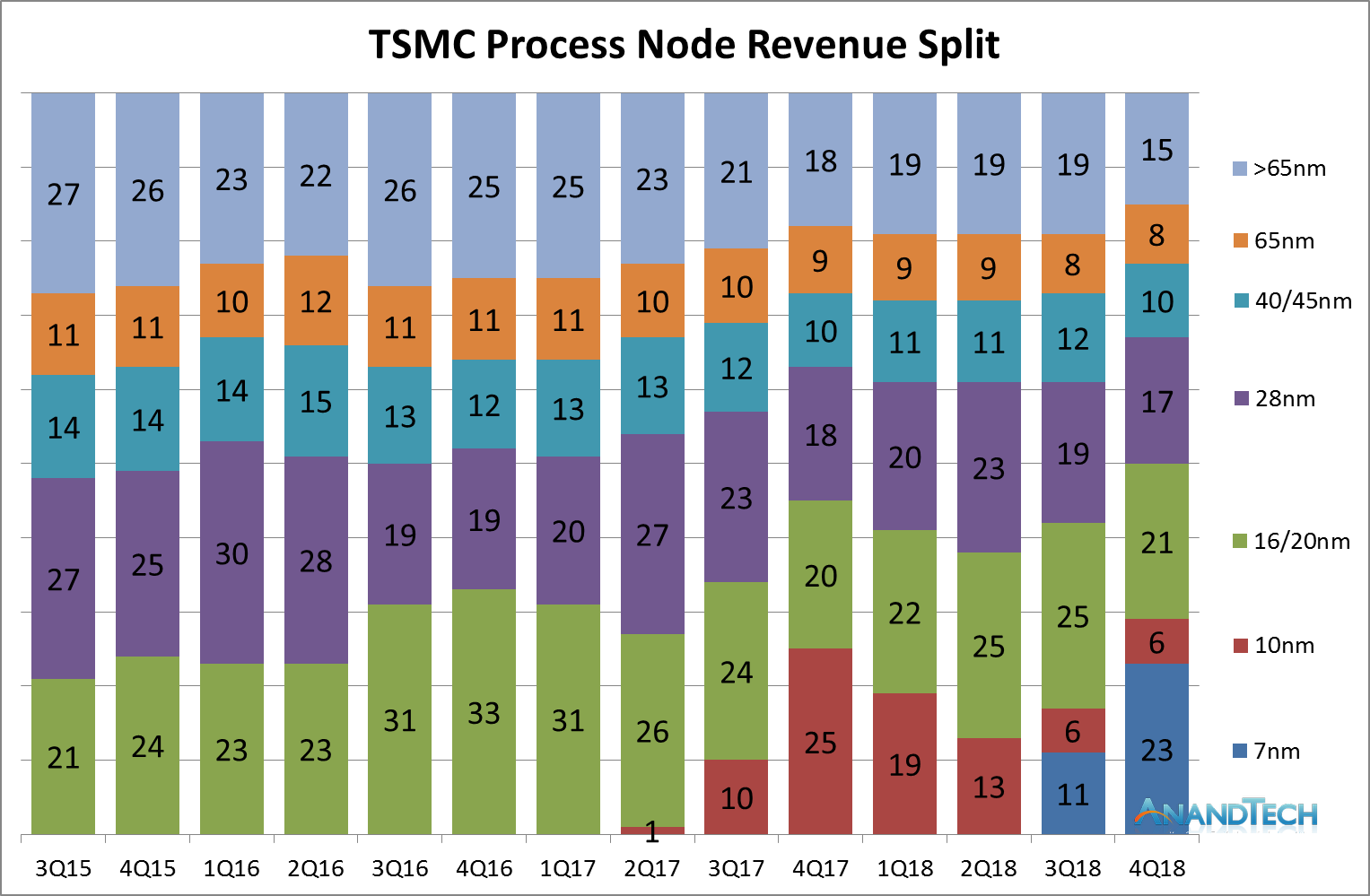
TSMC%20Tech.png


Even as of January 2019,TSMC 7nm only makes up 23% of their revenue and that is with everyone wanting to use it. So it could be that capacity is an issue for AMD. They have to make both CPUs and GPUs on TSMC 7nm as GF 7nm was cancelled.
 
Even as of January 2019,TSMC 7nm only makes up 23% of their revenue and that is with everyone wanting to use it. So it could be that capacity is an issue for AMD. They have to make both CPUs and GPUs on TSMC 7nm as GF 7nm was cancelled.

The most surprising thing in that image is how much of their revenue comes from >28nm, not so much the amount but that they're even still fabricating >28nm stuff, I mean wow who would've thunk it. :)

When i think of fabrication companies i automatically think cutting edge or a generation or two back from that, TIL.
 
That 7nm revenue is mostly Apple.
I don't see capo acity being a constraint for AMD; TSMC will be having Apple and Huawei producing large quantities of 7nm, but unlikely both at the exact same time, so AMD just needs the small amount above and beyond what those two need out of TSMC's overall 7nm capacity.
7nm will be a high volume node for sure, and costs will quickly come down I suspect.

The 14nm IO is clearly all about the WSA, which now only relates to 14nm wafers; AMD are free to use 7nm from anyone after the latest amendment.
 
Many structures that aren't cores don't scale well, as stated by AMD and 14nm is a well known, cost effective node. If you're not fighting for ultra low power and density isn't a main concern, there's no point in chasing the latest node.
 
Back
Top Bottom