

WikiChip has published their take on AMD’s upcoming Zen 2
https://fuse.wikichip.org/news/1815/amd-discloses-initial-zen-2-details/
Something to clarify
")
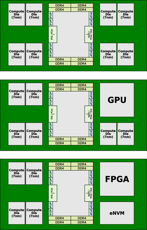
I/O Die
There is a lot of mystery surrounding the capabilities of the I/O die and AMD’s plan for the future. By moving all the “redundant components”, such as the I/O and southbridge, from the compute die to the I/O die, AMD has opened up their design to some intriguing possibilities. Since all the controls can be found in the centralized I/O die, it becomes possible to swap out the compute dies with other types of logic such an FPGA (e.g., from Xilinx) or a GPU. In Naples, this would have meant sacrificing some of the I/O or memory but with Rome, this is no longer the case. AMD has not announced any such plans, but the option is there.
")